Cracking the
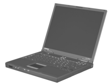
Compaq Evo N610c laptop
Introduction
The Compaq Evo N610c is a laptop that was released
in 2002. Compaq sold it with Windows XP and I was lucky enough
to be given a couple of them around 2013. These are my efforts
to "crack" one of them.
As I have other more modern laptops, I've used it
mainly to try out different flavours of GNU/Linux and for my Linux from
Scratch adventures. For those who don't know "Linux From
Scratch is a project that provides you with step-by-step
instructions for building your own customized Linux system
entirely from source." Deploying a GNU/Linux distribution this
way was kind of an eye opener: I only have the software that I
need installed, no one has dictated or imposed any so called
design decisions on me and, as a result, the computer runs
smooth, quick (with some exceptions: HD video, stupid
trashy bloated websites, etc.) Obviously, as everything
was compiled from source, it took me quite a long time to get
here. My desktop of choice is xfce for it's simplicity and ease
of use. I also have LibreOffice
for "words", "maths" and some image processing and Seamonkey for
Web browsing, email and html edition.
Motivation
As far as hardware goes these computers are very
solid, very robust and a pleasure to use. Both the keyboard and
the touchpad are great. (The pointing stick is, however, a bit
of dud in comparison.)
I'm using the computer to type this in and I find it quite
comfortable.
As a bit of history, both laptops worked almost daily for the
best part of 10 years. The only thing wrong with them was that
the hard drives needed to be replaced once. After 15 years, they
still works almost like the day they left the factory.
So, is there anything wrong with them? Sure, they have
Pentium4s, they get hot and spin the fans too often.
I realised I had all of this open source software
at my disposal. Given the inclination, I could analyse it all
and see how it all works.
It was then that it dawned on me, how about the
hardware? What else could I find out about this laptop? How
could I "crack it open" so that I could "see" how it works? How
far would I be able to go? What else would I be able to find
out?
Cracking it
Part 1 - The Internet search
Time to put the internet to good use and dive in.
I started by looking at some hardware specs the easy way:
HP (Compaq) has a great service
guide in their website.
My service tag states N610cP200X430VC250 UK so, from pages 7 and
8 I know I have a computer which originally had:
- Pentium 4 M at 2GHz
- XGA,1024 x 768 resolution 14" screen
- 30 GB hard drive
- DVD ROM
- MODEM / NIC combination card
- 256 Mb of RAM
- Windows XP Pro
Page 16 of the manual reveals that the battery is an 8 cell
4.0-Ah pack and that there are 32Mb of discrete video memory.
The computer came also with the operating system in CDROMs, with
a CD-RW drive, a floppy drive and an adaptor to connect the
floppy to the parallel port, which allows it to be used
simultaneously with any of the optical drives. All three drives
are easily replaceable in the drive bay as an option. There is
also the power supply.
All very good stuff back in 2003. At the time,
this was considered a great professional laptop from a good
brand. I have since upgraded the RAM to 2Gbytes and the hard
drive to 40Gbytes.
Let's find out more:
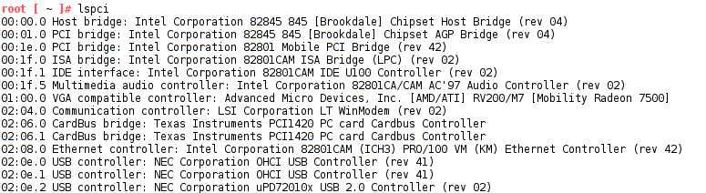
So now I know that I have a Brookdale chipset,
that the computer has an ATI Mobility Radeon 7500, an LSI
WinModem and a NEC USB 2.0 Controller
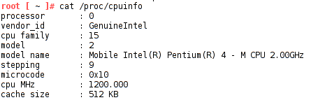
The processor is a Pentium 4 M capable of 2.00
GHz. (This I already knew.)
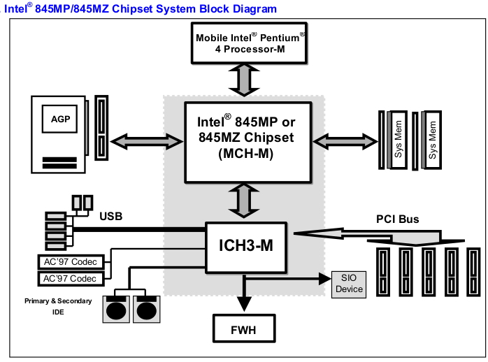
So, it was time to look for more information about all of these devices. It did not take me long to come across this diagram in the 82845 datasheet:
Lets look at all the datasheets I had this far
- Intel Pentium 4
M datasheet and specification
update
- IA32 Software Developer's Manual
Volume 1
- IA32 Software Developer's Manual
Volume 2
- IA32 Software Developer's Manual
Volume 3
(I have deliberately used the older versions
of these manuals here. The latest ones, which are backwards
compatible, are here.)
- Intel Pentium 4 Processor Optimization
Reference Manual
- Intel 82845
Memory Controller Hub (MCH-M) datasheet and specification update
- Intel
82801CAM I/O Controller Hub (ICH3-M) datasheet and specification update
- Texas Instruments PCI1420 PC Card
Controller
- NEC uPD720100A datasheet and manual
It was not possible for me to find the datasheet
for the Mobility Radeon M7 ATI graphics chip.
The closest I got was these manuals for the M6 which, I guess,
are close enough. Both the M6 and M7 are implementations of the
R100 chipset.
- Rage Mobility M6 Design guide
- Mobility M6 Pinout Specifications
- Mobility M6 Register
Reference Guide
- Rage
128 Software Developers Guide
This last file, although for a previous model,
goes into a lot of detail, describing the architecture of the
ATI cards.
It is targetted at BIOS and OS driver developers. The chip can
work in two distinct modes: VGA mode and Accelerator mode and
the manual describes the second mode. There's a very good
introduction to the way these cards work here.
For VGA, osdev.org provides a good explanation here. There is
also a detailed explanation here.
I decided not to look for information about the WinModem.
But this was obviously not enough. I still needed
to find out more.
Looking around, I could see an Infrared transceiver, a serial
port, a ps/2 mouse port...and, of course, the keyboard.
Part 2 - More Internet, a screwdriver and a bit
of luck
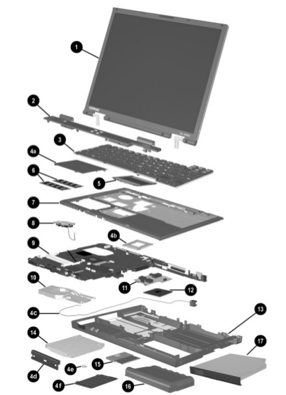
Time for some extreme measures... The excellent
Maintenance Manual tells you how to disassemble the laptop down
to the last screw so it was time to get the screwdriver and take
some pictures. It wasn't difficult.
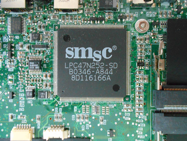
This revealed that the Super-IO chip is a SMSC LPC47N252. I managed to find the respective datasheet. This is where the keyboard controller, the serial, parallel and Infrared ports are.
The EEPROM with the firmware is a SST49LF008A. Hum... 1Mbyte.
The audio DACs are in a AD1886A chip feeding a LM4873 audio amplifier.
A few more datasheets:
ADM1032 Temperature Monitor
ICS950805 Frequency Generator
DA82562ET Ethernet LAN connect device
HDSL3602 IrDA Transceiver
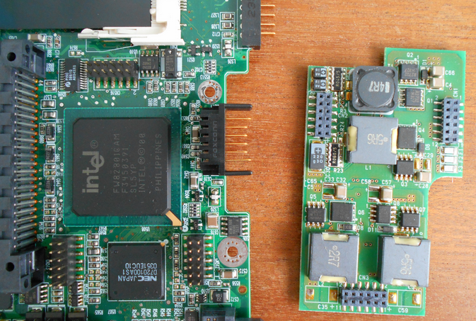
ISL6206 MOSFET Driver, ISL6215 Multi-Phase Buck PWM Controller and PI5C3861 10bit 2port bus switch
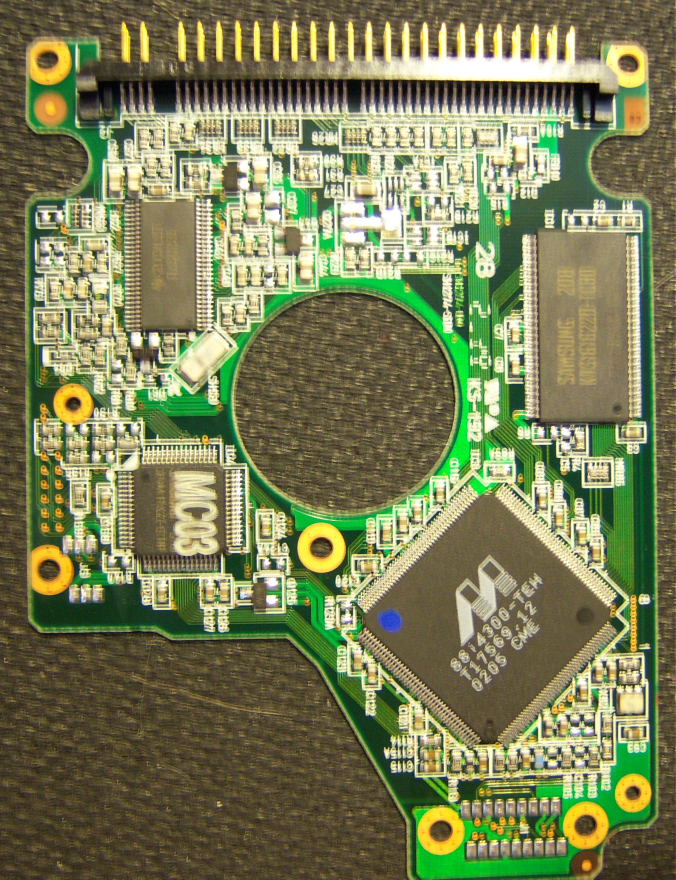
By the way, I also have an Hitachi Travelstar DK23DA-40 hard drive.
This drive seems to have a Marvell 88i4300 microcontroller inside, (not my picture.) Unfortunately it's close to impossible to find information about these chips. (Unless of course one uses extreme methods.)
The DVD-ROM drive has model number SD-C2612. It's a rebranded Toshiba part.
The CD-RW drive is a rebranded TEAC CD-W224E. I could not find any proper manual for it.
Let's go back and do a bit more digging in the command line.
Looking for some more information I decided to poke around the BIOS and did
root [ ~ ]# dd if=/dev/mem bs=1K skip=768 count=64 | strings -tx
where I found these strings
f346 Samsung LTN150P1-L02
f999 AUO B141XG03
So, my LCD is a AUO B141XG03-V2.
Towards the top there was this intriguing string
82 M7-P Compaq Fenway 2.0 BIOS ( 183/260MHz )
So I started looking for Compaq Fenway 2 and hit a bit of a jackpot (after a few hours of desperate internet surfing and muted cursing.)
Not only did I find out that the Original Design Manufacturer was INVENTEC but also the laptop's schematics.
Let's have a look at a better block diagram from the schematic diagram's pages and continue the quest.
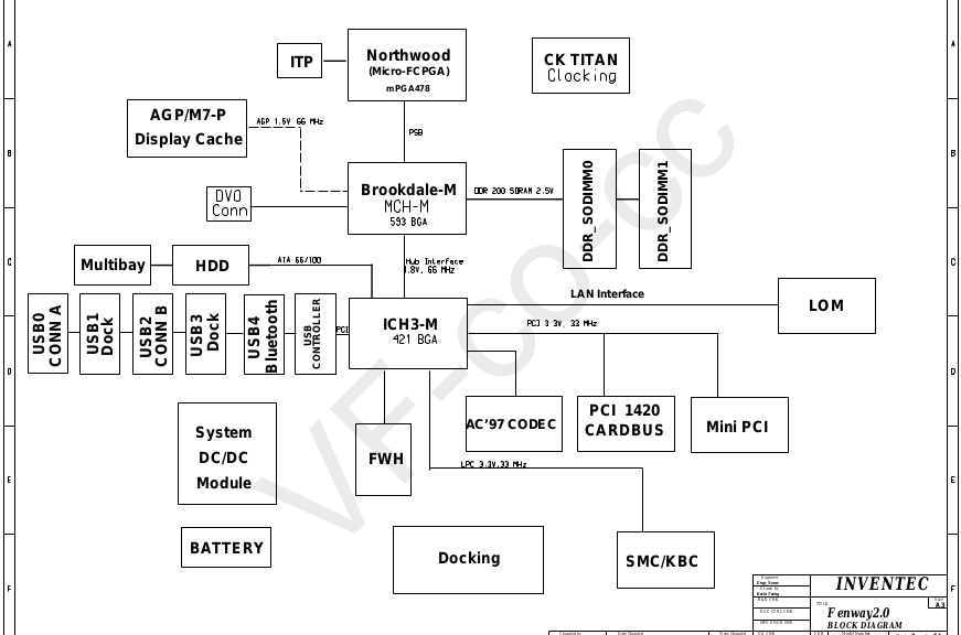
For those of you unfamiliar with computer schematic diagrams, and/or who don't know electronics, they are actually easy to follow with a few simple rules:
- The small downward triangles connect to the ground, imagine this is the - terminal in a battery. This is zero voltage and represents "logical zero"
- The circles are positive voltages, i.e. per analogy, the + sign in a battery, they represent "logical ones".
- Ignore all the capacitors. I marked them red below
- Think of all the resistors below 10K as short circuits, as direct connections, as a wire between the two points. I marked them in green. Same with the diodes, which look like arrows painted dark on the inside.
- Think of the resistors with 10K or above values as "pull ups" or "pull downs". Example in blue. They are there to give the line a default value of either logical one or logical zero respectively. The line can still be brought low or high by the rest of the circuit.
- Some lines are actually "three state". They can be logical high, logical zero or high impedance. High impedance means that the pin of the chip connected to the line behaves like it is not connected at all. Sometimes this is why there are the pull ups and pull downs as usually, input pins don't like to have nothing connected to them.
- The arrow symbols mean that the the line continues on another page of the schematic. The page numbers are there, next to them. Sometimes they define a "direction" which can help us know which pins are outputs and which ones are inputs.
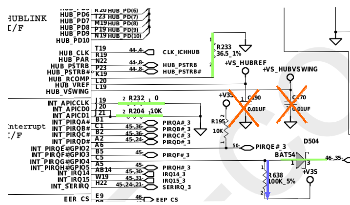
So now, not only did I have details about practically all the hardware in the computer, I also knew how they were all connected with each other.
Part 3 - Standards
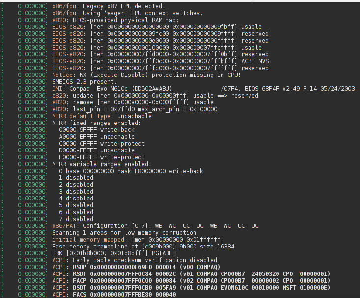
So, the dmesg command shows me the kernel detecting my memory,
my hardware and joyfully use it to great effect. Here are the first few lines...
But, how does it know where to look? The short answers is that it comes from the BIOS. This is where a number of specs come into play.
The specs define the way the BIOS prepares the system to be taken over by the operating system. The way it all works is complicated mainly due to the need to maintain backwards compatibility but also to be able to make available the latest technologies that give us more speed, more power and allows us to extract more usability out of our computers. (i.e. higher quality cat videos.)
There are two very important aspects about this laptop: the first one is that it is ACPI 1.0b compliant and the second is that it is PCI 2.2 based.
From a software point of view, ACPI defines a standardized ways for the operating system to communicate with the hardware and assists it in all the power aspects, i.e. sleep, hibernate, shutdown, power off, etc. The way this is done is explained very well in the OSDev.org website here. Before continuing I recommend reading it. The introduction sections of the specs are also quite good.
ACPI is much more than a sw specification. It affects all aspects of the computer design. The whole circuit and all the chips in it now have to be aware of the different power states.
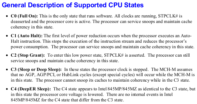
The MCH-M datasheet, in section 5.4 has a relatively good description of the various states the system can be in. Both the ICH3-M and Super-IO datasheets contain more information.
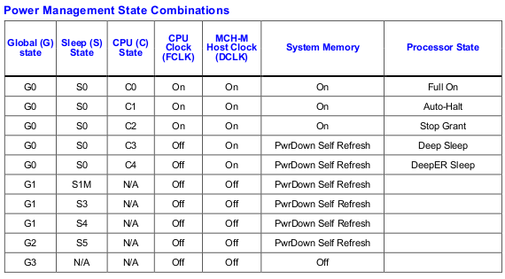
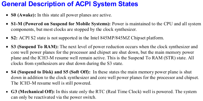
It's important to be aware of these concepts when looking at the computer schematics.
Page 3 has this diagram which shows us how the voltages inside the computer are switched on and off.
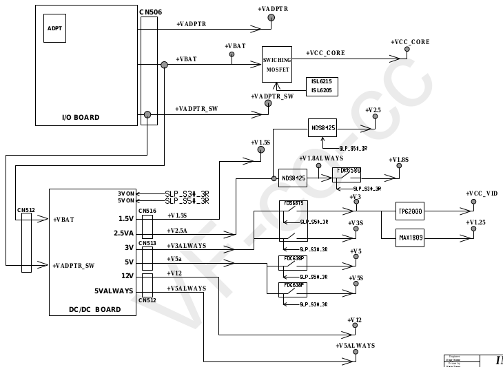
Not only are the voltages affected, the ICS950805 frequency generator also needs to adapt to the different power states.
So, what happens when one presses the power button? Hum... Lets go back even further...
Lets imagine for a start the laptop without any power source. You start by putting in the CR1220 cell battery. This will start the RTCs (real time clocks) on the ICH3-M and the Super-IO chips running. The NVRAMs in both chips will now also keep their contents.
Then, you place an empty main battery in the laptop. Nothing much happens.
Now you connect the power adaptor. At this stage, the 8051 inside the Super-IO starts running code. It will always be the 8051 which will be responsible for most of the power aspects of the whole computer. It controls the on/off of most voltages, measures the temperatures and spins the fan. It works together with the ICH3-M.
The Pentium 4 M doesn't really directly control any aspects of the laptop. Looking at the datasheet and the schematic, we see that the Address, Data and Control (REQ) lines all connect only to the MCH-M. This is the only way that the processor has to talk with the outside world... The MCH-M is a chip which contains the PCI bridges needed to connect the processor to the memory, to the video card and to the rest of the peripherals. The video card interface is AGP, which is a special kind of PCI. The "rest" is the ICH3-M chip, to which it connects by a proprietary interface. The PCI configuration devices inside the MCH-M, configure the address ranges the bridges will use to forward the memory and IO accesses to either the video or ICH3-M.
There is a very good explanation about PCI at the OSDev.org website here. It's recommended reading at this stage.
The ICH3-M, on the other hand, besides all the devices inside it, also has a ISA bridge, which is used to forward IO accesses to the Super-IO chip through the LPC (Low Pin Count) physical bus and memory accesses to the FWH (the EEPROM chip where the BIOS code is kept).
(Here are the LPC specifications for reference. Reading not required at this stage.)
Other legacy functions are also taken care of by this PCI device, like the RTC, the DMA controller, Interrupt Controller and Timers. Proper defaults guarantee that, upon power on, the computer looks from a software point of view, like a regular ISA PC so, older operating systems, not aware of PCI or ACPI can still continue to run.
The backwards compatibility of the PC platform has always been one of its most endearing characteristics.
In a way, this laptop is the perfect study object, as it comes from a time that married the old ISA (and Plug&Play) computers with the more modern ACPI / PCI ones of today. Both ACPI (as of May 2018 the current version is 6.2) and PCI (PCI Express revision 4) have evolved, but are still basically very similar to the specs that I attached above.
The main big developments my documentation does not cover are the shift to 64bit architectures, Multiprocessor/Multicore systems, the AHCI SATA PCI devices, the infamous chipset Management Engine (ME) and, of course, the move away from the BIOS to UEFI.
For the sake of completeness here are a few more specs.
hdparm shows that my dive is ATA-5 rev3 compliant.
A very good introduction to ATA can be found here. This is not required reading at this stage.
ATA-5 Command set rev3
ATA-8 Parallel interface
A cool intel programmers reference manual for the IDE controller in the ICH3 is here.
Part 4 - The soft bits
With all those documents, I now had a very good chance of understanding most of the hardware. I was surprised about how many of them are actually either publicly available or "not impossible" to find indexed in internet search engines.The equipment manufacturers actually do a relatively bad job of keeping documentation for these old parts, extreme thanks need to go to archive.org.
Had I finished my quest? Was I now able to completely understand my laptop, given the inclination, in the same way I could understand my software? What was I still missing?
If a software quest can start at the way a computer boots, (recommended reading here) then I still had some work to do.
I wanted to understand more about the BIOS and how it delivered the Compaq to the operating system.
So I started from the bottom and took a better look at the Super-IO Chip. There's a neat diagram below. This whole chip is more complicated than a lot of early 80's 8 bits microcomputers. It is a whole fully fledged computer in its own right.
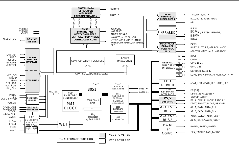
(VCC0 comes from the cell battery, VCC1 exists whenever there is a charged battery or a charger connected and VCC2 is a commuted voltage that is present when the computer is on.)
Through the use of its extensive number of general and special purpose pins, this chip controls practically all the aspects of the motherboard. In a way, this chip has the "power" and the "brains" to make all of the other chips nothing more than puppets. Yes, this includes the Pentium 4 M. :)
The LPC47N252 datasheet is quite well written but has a few issues. It took me quite a few reads because of that.
In order to understand this chip, you have to read it in a slightly skewed way:
- Start off with this generic Intel 8051 manual. Only chapter 1 is required, chapter 2 may be referred to later.
- Then, go back to the LPC47N252 datasheet and read section 11 up to page 132.
- Read the whole of section 31 and appendix A
- Now read Section 13 up to and including section 13.5, then 13.11
- Finally, Section 19 up to and including 19.6
At this stage, I felt that I was ready to read the EEPROM of the Super-IO chip.
I'm not a great programmer and so I was only able to came up with that below. I never managed to "properly" stop the 8051 processor and the watchdog timer would reset it, powering off the whole computer after the program ran. The way I eventually worked around it was to issue a sync linux command right after the program did it's work.
#include <stdio.h>
#include <sys/io.h>
#include <sys/types.h>
#include <unistd.h>
#include <fcntl.h>
int print_addr(u_int8_t log_device) {
u_int8_t tmp[256];
u_int8_t flash[65536];
outb_p(0x07,0x2E); outb_p(log_device,0x2F);
outb_p(0x60,0x2E); tmp[3]=inb(0x2F); // Register 0x60
outb_p(0x61,0x2E); tmp[4]=inb(0x2F); // Register 0x61
printf("Logical Device %d address = %04X\n",log_device, (tmp[3] << 8) | tmp[4]);
return (tmp[3] << 8) | tmp[4];
}
int main () {
int x, i, j;
int fd;
ioperm(0x2E,8,1);
ioperm(0x2F,8,1);
ioperm(0x80,8,1);
outb_p(0x55,0x2E); // Enter configuration mode
outb_p(0x26,0x2E); tmp[1]=inb(0x2F);
outb_p(0x27,0x2E); tmp[2]=inb(0x2F);
printf("\nLPC Address %04X\n\n",(tmp[2] << 8) | tmp[1]);
printf("FDC ");print_addr(0);
printf("PM1 ");print_addr(1);
printf("Parallel ");print_addr(3);
printf("Serial ");print_addr(4);
printf("Infrared ");print_addr(5);
printf("RTC ");print_addr(6);
printf("KBD ");print_addr(7);
printf("ACPI EC ");print_addr(8);
printf("Mailbox ");x=print_addr(9);
printf("GPIO ");print_addr(10);
ioperm(x,16,1);
for(i=0x80;i<0xb0;i++) {
outb_p(i,x); tmp[1]=inb(x+1);
printf("%02X %02X\n",i,tmp[1]);
}
outb_p(0x97,x); outb_p(0x08,x+1); // Disable SMI Interrupts
outb_p(0x94,x); while ((inb_p(x+1)&0x80) ==0 ) ; // Wait for Idle 8051
outb_p(0x94,x); outb_p(0x01,x+1); //stop 8051 clock
outb_p(0x9E,x); outb_p(0x12,x+1); // enable Host eeprom read
outb_p(0x80,x); tmp[20]=inb(x+1); //save for later
outb_p(0x9F,x); tmp[21]=inb(x+1); //
for(i=0;i<=255;i++) {
for(j=0;j<=255;j++) {
outb_p(0x9F,x); outb_p((u_int8_t) i,x+1);
outb_p(0x80,x); outb_p((u_int8_t) j,x+1);
outb_p(0x81,x);
tmp[0] = inb_p(x+1);
// printf("%04X %02X\n",i<<8|j,tmp[0]);
flash[i<<8|j] = tmp[0];
}
}
outb_p(0x80,x); outb_p(tmp[20],x+1); //re-instate values
outb_p(0x9F,x); outb_p(tmp[21],x+1); //
outb_p(0x9E,x); outb_p(0x10,x+1);
outb_p(0x94,x); outb_p(0x00,x+1);
outb_p(0x97,x); outb_p(0x00,x+1); // Enable SMI Interrupts
/* for(i=0;i<256;i++) {
for(j=0;j<256;j++) {
printf("%02X",flash[i<<8|j]);
}
}
*/
// printf("\n %02X %02X %02X %02X \n",tmp[1],tmp[2],tmp[3],tmp[4]);
// Exit Configuration mode
outb_p(0xAA,0x2E);
if((fd = open("/root/flash.bin",O_WRONLY|O_CREAT)) == -1) {
printf("\nError file open\n");
}
else {
if(write(fd,&flash[0],65536) != 65536) printf("\nWrite Error\n");
close(fd);
}
}
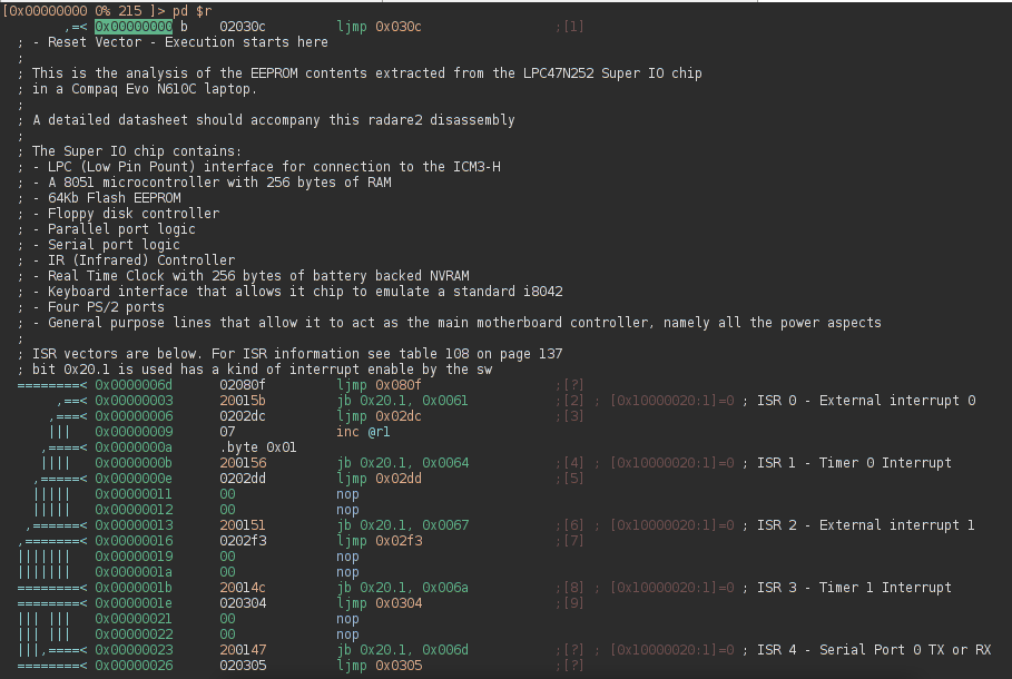
So, here is the result... the 8051 FLASH Contents.
I've starting analysing it with radare2 and it is hard work. The main limitation here is time, which never seems to be enough...
I have changed the 8051_disas.c file in libr/asm/arch/8051/ to take into account the differences in special function registers between the 8051 in the Super-IO chip and the regular 8051 family.
The next step was to have a good look at the BIOS.
The schematic diagram shows that the BIOS EEPROM chip (a.k.a. FirmWare Hub) is connected to the rest of the system (actually the ICH3-M) by the LPC bus. The ICH3-M does address translation on its PCI to ISA bridge. There is a PCI configuration register in this device that allow us to better understand this mapping.
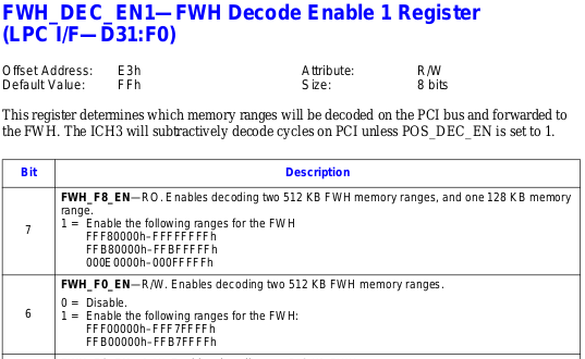
So, I had a look at it. It's at offset E3h in the PCI configuration space.
root [ ~ ]# lspci -s 00:1f.0 -xxx
00:1f.0 ISA bridge: Intel Corporation 82801CAM ISA Bridge (LPC) (rev 02)
00: 86 80 8c 24 0f 01 80 02 02 00 01 06 00 00 80 00
10: 00 00 00 00 00 00 00 00 00 00 00 00 00 00 00 00
20: 00 00 00 00 00 00 00 00 00 00 00 00 00 00 00 00
30: 00 00 00 00 00 00 00 00 00 00 00 00 00 00 00 00
40: 01 10 00 00 10 00 00 00 00 00 00 00 00 00 00 00
50: 00 00 00 00 00 00 00 00 01 11 00 00 10 00 00 00
60: 0b 0b 0b 0b 92 00 00 00 0a 80 80 80 00 00 00 00
70: 00 00 00 00 00 00 00 00 00 00 00 00 00 00 00 00
80: 00 00 00 00 00 00 00 00 00 00 00 00 00 00 00 00
90: fd 54 00 00 00 00 00 00 00 00 00 00 00 00 00 00
a0: 2d 03 00 00 02 00 00 00 0d 00 00 00 00 00 00 00
b0: 00 00 00 00 00 00 00 00 0a 41 82 05 00 00 00 00
c0: 30 00 00 00 40 01 00 01 00 00 00 00 7f 00 00 00
d0: 07 20 00 02 02 0f 00 00 04 00 00 00 00 00 00 00
e0: 70 00 00 c0 00 00 0f 3c 33 22 11 00 00 00 67 45
f0: 00 00 49 87 00 00 00 00 47 0f 0f 00 00 00 81 00
C0 hex = 11000000 in binary which means that bits 7 and 6 are 1 and the memory ranges in the datasheet map to the FWH.
Time for me to write another one of my "wonderful" programs... (cough cough did I say write? I just copied it from somewhere...)
#include <unistd.h>
#include <stdio.h>
#include <fcntl.h>
#include <assert.h>
#include <sys/mman.h>
int main() {
char *mem;
int fdi,fdo;
fdi = open ("/dev/mem", O_RDONLY);
assert(fdi >= 0);
mem = mmap( NULL, 512*1024, PROT_READ, MAP_SHARED, fdi, (off_t) 0xFFB00000);
assert(mem != MAP_FAILED);
printf("Memory pointer: %p\n", mem);
fdo = open("/root/fwh.bin",O_WRONLY|O_CREAT);
assert(fdo >= 0);
write(fdo,mem,512*1024);
munmap(mem, 512*1024);
close(fdi);
close(fdo);
return 0;
}
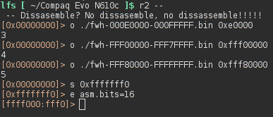
Changing the address in the mmap call I extracted all the contents of the 5 areas.
For the sake of completeness I also got the Video BIOS and the Option BIOS areas using the traditional method:
dd bs=1K count=128 skip=768 if=/dev/mem of=video+option.bin
The option area, "optionally" contains code that allows the computer to boot from the ethernet card.
Code is only present there if chosen in the BIOS screens.
You can find them zipped here.
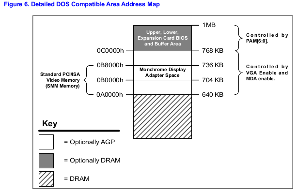
But, if we have a 1Mbyte EEPROM how can there be four 512Kbyte areas and another 128Kbyte?
The first explanation is here in the datasheet:
So, the whole address range 0xFFB00000-0xFFBFFFFF is there so that the system can access the few memory mapped registers of the flash chip.
The second is a bit more complicated. The 0x000E0000-0x000FFFFF range is there to give the system manufacturers the option to build systems where the "normal" BIOS, which resides at these addresses to be the same code that is kept also at the 0xFFFE0000-0xFFFFFFFF addresses.
In practice, this never happens; during the computer start up the whole memory area between 0x000A0000-0x000FFFFF is "dynamically" written to RAM (which is much faster) by the code and then protected by the PAM and SMM register mechanisms in the MCH-M chip.
The reason I say dynamically is because what you will find in this area will vary depending on the options you chose in the BIOS configuration screens. (Those accessible by pressing F10 after power up.)
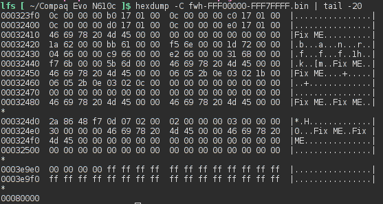
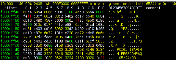
(Hexdumping one of the 512Kbyte shows that it is pretty empty towards the end. I find those "Fix ME"s really funny.)
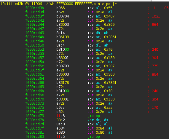
Running the strings command on the files is also quite interesting.
It is also not easy to find information about the BIOS on the internet. This is quite surprising considering how beaten the PC platform is. There are some good exceptions though, like this excellent book.
The book goes through great detail, describing the structure of the Award and AMI BIOS, which are the most common. Compaq, however does their own thing.
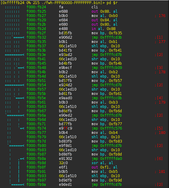
Radare2 is able to disassemble the BIOS files too and is clever enough to know that the 128Kbyte file is a BIOS, "out of the box".
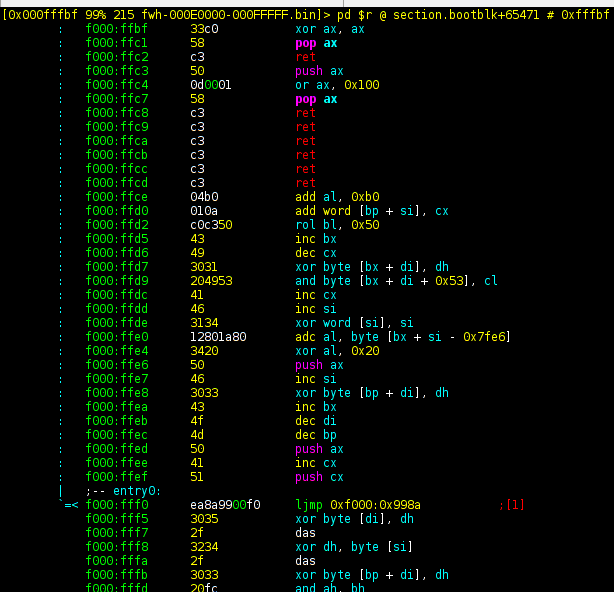
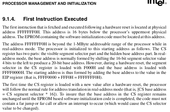
However, in reality, the first instruction executed is not in that part of the BIOS. Let's read this carefully from Volume 3 of the intel developer manuals
Let's then do this properly
Going to visual mode we can see a jump where we expect it to be and a nice date string below
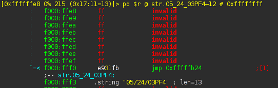
Following the code
And some of the first instructions look rather familiar, i.e. are "out" instructions to port 0x2E, the Super-IO configuration address.
Part 5 - The End
At this point, I'm content. I have reached my objective and answered my original question. Given the inclination, "I can" actually analyse the hardware and see how it all works.
I hope you have enjoyed this. If you have, and got curious, can you also "crack" your own computer?
------------------
( Disclaimer: As far as I know, all the information I make available here is public and not subject to any publication restrictions. If this is not the case, please email me at compaq(a.t.)edbatalha.info )
