20-August-2019
Compaq EVO N610c bugs
Introduction
Strictly speaking these are not really bugs, these are/were just
some things bugging me. I managed to solve most of them, at least
up to a level that I'm happy with. Here's the list:
1) Back-light control - Solved
There is no back-light control in the linux
kernel for this computer. No matter what kernel choices I chose
nothing worked.
2) SPD memory - Solved
RAM DIMMs have a small eeprom chip with details
regarding how the memory controller is to be configured to work
with the RAM. Usual internet knowledge just tells you to run the
decode-dimms command. Nope, not working here buddy.
3) System EEPROM - Still a bugger
On page 22 of the schematics there is an eight
legged creature labelled "System EEPROM". What the frack are you
and what are you doing there?
4) There is a debugger in my
BIOS and I like catching bugs. How do I use it?? - Solved
5) To spin or
not to spin, that is the question - Solved
I was always puzzled by the threshold
temperatures chosen by Compaq to spin the fan. Could I do
something about it?
6) "Stupid square thingy"
- Solved
The lack of "proper" documentation for the
graphics chip really bothered me. Could I find a way to control it
myself?
7) "Stupid square
thingy" slow and steady - Solved
Another take on the stupid square, this time
let's take it slow.
8) FreeDOS and a real PCI BIOS bug this
time - Solved
(You'll need to read the Compaq
N610c page first before continuing.)
Back-light control
Part 1)
So, what is the motivation? Believe it or not, the screen is just
too bright to work at night in a very dimly lit room. I understand
that a bright screen is useful when you're working in an office,
by the window, in a sunny country, overlooking the beach (dream
on...) so we cannot fault AUO for doing this. On the contrary, a
big thanks to you AUO.
(By the way, there are some great animations
on their site.)
Indeed, I know that it is possible to just type:
$ xrandr --output LVDS --brightness 0.5
at the prompt to reduce the brightness to half, but this feels
like cheating because all that this command is doing is making all
the pixels darker, i.e. you have a bright light behind and get the
liquid crystal to hide it. The cheat can also be seen in the mouse
cursor, which remains bright.
So, I knew that removing the charger changes the "proper"
brightness and what this means is that:
- The LM2601 adapter interface chip
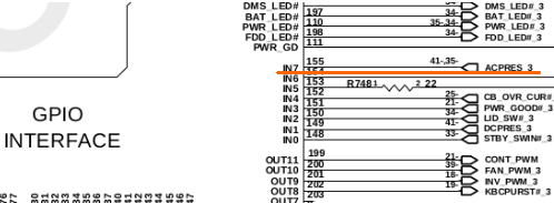
senses the power change and changes the ACPRES_3_IO signal
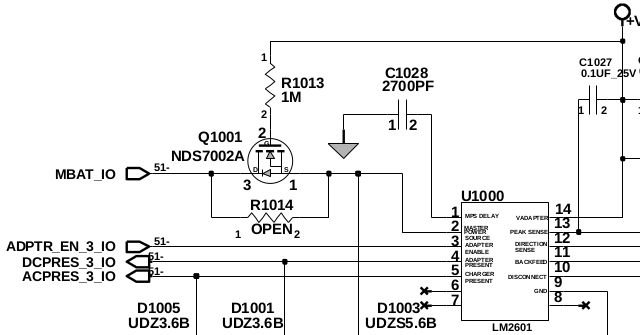
- That signal ends up in the Super-IO controller's pin 155, aka
IN7
(The trick here is to know that connector CN1002 is the other side
of connector CN501)
- The Super-IO is configured to react to changes on this pin and
its interrupt routines then raise a SCI to the Pentium 4 and
operating system
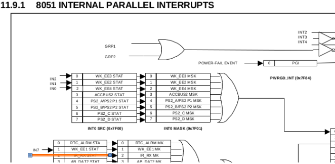
Now, a SCI is a System Control Interrupt and is described in the
ACPI specifications this way (quoting from the specs):
"A system interrupt used by hardware to notify the OS of ACPI
events."
So, what does the almighty internet have to say about all of
this?
The theory goes that when such an interrupt is received, the
kernel will look for the device that generated the interrupt, get
the event number, look in the ACPI tables that the BIOS made
available for the code and that has instructions regarding what to
do and then execute them.
Could I then see all this process in action?
Well, I ended up going to the ACPICA downloads page,
downloading the code and following the instructions to make the
package and generate the utilities.
Then all that was left was running them in the right order
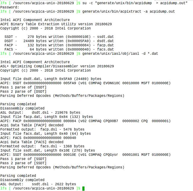
The process above dumps the ACPI tables that the linux kernel is
aware of to a file, then separates that file into the 4 component
tables and disassembles them to four .dsl files with source code
in the ASL language.
Bar variable names, these files are copies of the source code that
compaq compiled, placed in the bios and which regulate the ACPI
functionality of the laptop. So, we have a bit more than 200K of
code to go through.
Blog posts like this and this are
really good but, did I really need to learn a new programming
language just to change the back-light? As this looked tedious and
time consuming I tried another way, made a mental note to return
to this subject later and carried on.
Part 2)
There is a small note in the LCD datasheet like this:

The inverter is the circuit needed by the system to generate the
high voltages required by the CCFL (Cold Cathode Fluorescent
Light) i.e. the back-light. The note implies that the brightness
may be controlled by PWM.
PWM stands for Pulse Width Modulation. In the most common use, it
refers to "square signal" waves or clocks where the time the
signal is on may be different from the time it is off. There is
usually a percentage value associated called duty cycle.
On page 18 of the schematic diagram we find the LCD connector and
there is, indeed, a line there called INV_PWM_3
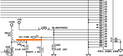
Since it goes to page 21 then it must connect to the Super-IO
chip...
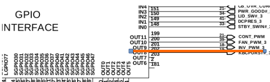
... and so it does, to pin 201 aka OUT9.
This pin can be configured to be the result of the PWM2 Function.
(Datasheet typo bonus, can you spot it?)
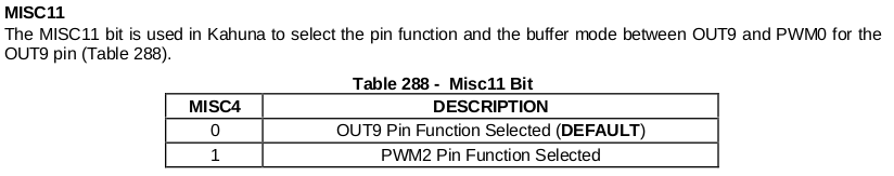
The whole of Chapter 20 in the datasheet is dedicated to the
programmable Pulse Width Modulators.
It's just 3 pages, mostly tables and the most relevant information
is here.
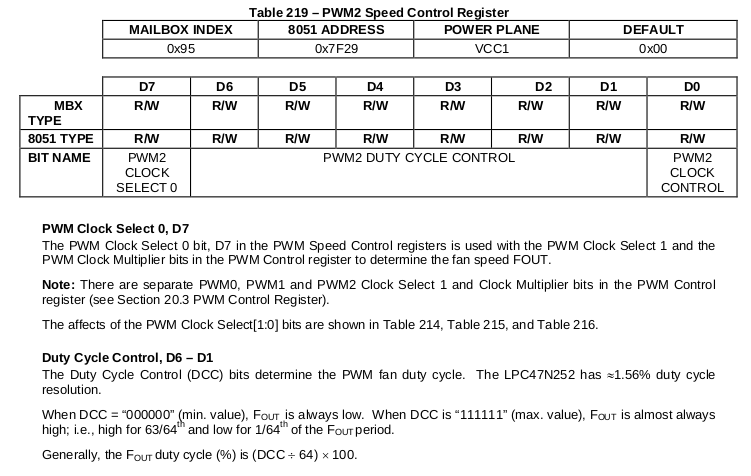
Note that this is also a Mailbox indexed Register and that I had
encountered these before, when I read the eeprom of the 8051.
So I made another one of my extremely stupid programs, a proof of
concept that "just works".
#include <stdio.h>
#include <sys/io.h>
#include <sys/types.h>
#include <unistd.h>
#include <fcntl.h>
u_int8_t tmp[8];
int print_addr(u_int8_t log_device) {
outb_p(0x07,0x2E); outb_p(log_device,0x2F);
outb_p(0x60,0x2E); tmp[3]=inb(0x2F); // Register 0x60
outb_p(0x61,0x2E); tmp[4]=inb(0x2F); // Register 0x61
printf("Log Dev %d address = %04X\n",log_device, (tmp[3]
<< 8) | tmp[4]);
return (tmp[3] << 8) | tmp[4];
}
int main () {
unsigned int x, y;
ioperm(0x2E,8,1);
ioperm(0x2F,8,1);
ioperm(0x80,8,1);
outb_p(0x55,0x2E); // Enter configuration
mode
outb_p(0x26,0x2E); tmp[1]=inb(0x2F);
outb_p(0x27,0x2E); tmp[2]=inb(0x2F);
printf("\nLPC Address %04X\n\n",(tmp[2] << 8) |
tmp[1]);
printf("Mailbox ");x=print_addr(9);
ioperm(x,16,1);
printf("Changed to 90%\n"); y=0x80|(( 56 )<<1);;
outb_p(0x95,x); outb_p(y,x+1);
getchar();
printf("Changed to 80%\n"); y=0x80|(( 50 )<<1);;
outb_p(0x95,x); outb_p(y,x+1);
getchar();
printf("Changed to 70%\n"); y=0x80|(( 44 )<<1);;
outb_p(0x95,x); outb_p(y,x+1);
getchar();
printf("Changed to 60%\n"); y=0x80|(( 37 )<<1);;
outb_p(0x95,x); outb_p(y,x+1);
getchar();
printf("Changed to 50%\n"); y=0x80|(( 31 )<<1);;
outb_p(0x95,x); outb_p(y,x+1);
getchar();
printf("Changed to 40%\n"); y=0x80|(( 25 )<<1);;
outb_p(0x95,x); outb_p(y,x+1);
getchar();
printf("Changed to 30%\n"); y=0x80|(( 19 )<<1);;
outb_p(0x95,x); outb_p(y,x+1);
getchar();
printf("Changed to 20%\n"); y=0x80|(( 13 )<<1);;
outb_p(0x95,x); outb_p(y,x+1);
getchar();
printf("Changed to 10%\n"); y=0x80|(( 6
)<<1);;
outb_p(0x95,x); outb_p(y,x+1);
getchar();
printf("Changed to 00%\n"); y=0x80|(( 0
)<<1);;
outb_p(0x95,x); outb_p(y,x+1);
getchar();
printf("Back to 100%\n");
outb_p(0x95,x); outb_p(0xfe,x+1);
// Exit Configuration mode
outb_p(0xAA,0x2E);
}
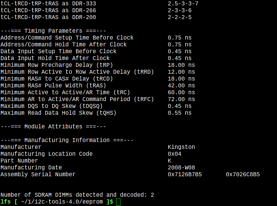
SPD Memory
In my quest
to learn more about this laptop there came a time when I decided
to know some more about the RAM memory. What RAM did I really
have, what were the specs, etc, etc...
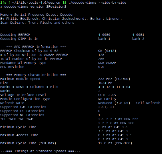
In all it's cleverness, all that the internet would tell me was to
use the command 'decode-dimms' from the i2c-tools
package. Obviously, it did not work...
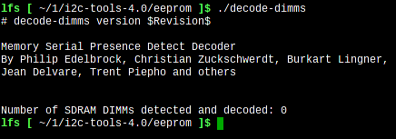
Then, the internet blurted... You're an idiot, you need to have the
eeprom driver in your kernel.
And so I did, I compiled my kernel with this driver. But
'decode-dimms' was still not working.
The man page for 'decode-dimms' states it is a tool "to decode the
information found in memory module SPD EEPROMs."
But, what is SPD? Aren't we talking about RAM?
SPD stands for Serial Presence Detect and is a small EEPROM chip
that exits in all memory modules since the mid nineties. Wikipedia
has a very nice article
about it and for me the two key sentences were these:
"The SPD EEPROM is accessed using SMBus,
a variant of the I²C protocol. This reduces the number of
communication pins on the module to just two: a clock signal and a
data signal."
Looking at the schematic we can see the signals in the Dual Inline
Memory Module connector pins 195 and 193:
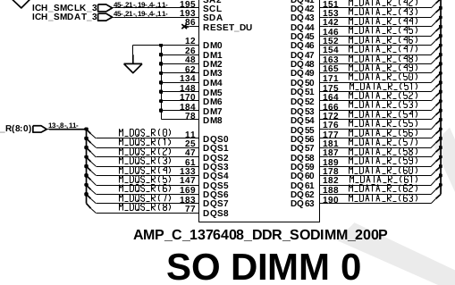
Which leads us to page 19 and to the corresponding pins in the
ICH3-M.
Sub-chapter 5.17 and chapter 12 describe this device in detail.
Quite helpful also, for reference, is the applicable SMBus standard.
So now I knew I also had to include some more stuff in the kernel
This option needed to be selected...
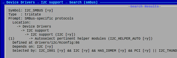
...along with this one
Another reboot later... Did it work?
Nope. The manual says I should see a 00:1f.3 device but it's just
not there
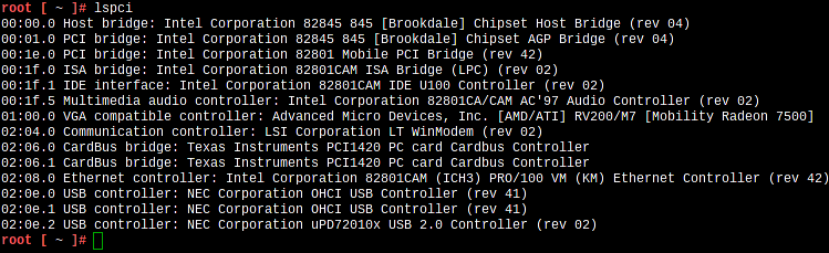
What was I doing wrong? Would I ever figure it out???
Something must be wrong with the driver, right? Actually with the
whole PCI enumeration stuff.
So I checked the linux kernel documentation. There's a file called
'i2c-i801' in the Documentation/i2c/busses/ folder which states
this...
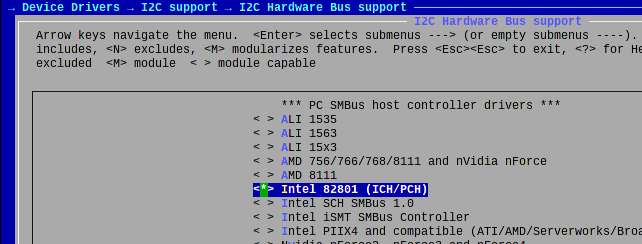
Hidden ICH SMBus
----------------
If your system has an Intel ICH south bridge, but you do NOT see
the
SMBus device at 00:1f.3 in lspci, and you can't figure out any way
in the
BIOS to enable it, it means it has been hidden by the BIOS code.
Asus is
well known for first doing this on their P4B motherboard, and many
other
boards after that. Some vendor machines are affected as well.
The first thing to try is the "i2c_ec" ACPI driver. It could be
that the
SMBus was hidden on purpose because it'll be driven by ACPI. If
the
i2c_ec driver works for you, just forget about the i2c-i801 driver
and
don't try to unhide the ICH SMBus. Even if i2c_ec doesn't work,
you
better make sure that the SMBus isn't used by the ACPI code. Try
loading
the "fan" and "thermal" drivers, and check in /proc/acpi/fan and
/proc/acpi/thermal_zone. If you find anything there, it's likely
that
the ACPI is accessing the SMBus and it's safer not to unhide it.
Only
once you are certain that ACPI isn't using the SMBus, you can
attempt
to unhide it.
In order to unhide the SMBus, we need to change the value of a PCI
register before the kernel enumerates the PCI devices. This is
done in
drivers/pci/quirks.c, where all affected boards must be listed
(see
function asus_hides_smbus_hostbridge.) If the SMBus device is
missing,
and you think there's something interesting on the SMBus (e.g. a
hardware monitoring chip), you need to add your board to the list.
I looked at this and thought, wow, this is scary. I don't want to
unhide the controller and destroy the computer due to over heating.
I decided to drown my frustrations on something else, maybe some
inspiration would come...
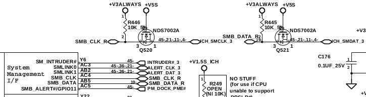
I picked up the schematic diagram again and played a game of spot
the bus. SMBus is just a special case of the I²C and I found many of
these in the motherboard.
The Super-IO has two I²C controllers, each controlling a pair of
buses by means of multiplexing. The datasheet calls them ACCESS.Bus.
I have no idea why... Here is the specification
if you're interested.
Following the bus lines on the schematic diagram we see that these
devices connect to the Super-IO chip:
- A system EEPROM (page 22)
- A thermal sensor for the CPU (page 39)
- The main battery (page 40)
- The extra battery, that can be installed in the cd-rom, floppy bay
(page 40)
- The docking station connector (page 35)
- The mini-pci connector (page 36)
These devices connect to ICH3-M:
- The SO-DIMM memory connectors
- The ICS950805 Frequency Generator chip
The M7 ATI Radeon chip has independent I²C buses for
- LCD, VGA and DVI connectors
In this case the I²C bus is "renamed" DDC.
So, actually, the ICH3-M's SMBus only talks to the memories and to
the Frequency generator chip. Reading the manual of this chip my
understanding was that it is only programmed by ACPI when the
computer needs to suspend or hibernate.
Back to the ICH3-M datasheet I found this register
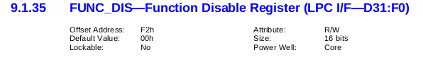
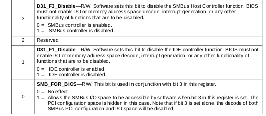
I felt like I was finally getting somewhere. Let's see...
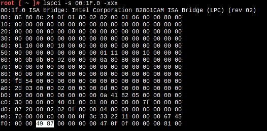
0x8749 = 1000 0111 0100 1001
So, bit3 is 1, the device is disabled and bit0 is 1, meaning that
the IO space was left enabled.
Time to write another one of my programs...
The program clears bit 3 and then reads the PCI configuration space
of the SMBus device which should now be visible.
#include <stdio.h>
#include <sys/io.h>
#include <sys/types.h>
u_int8_t pciConfigReadByte (u_int8_t bus, u_int8_t slot,
u_int8_t func, u_int8_t offset)
{
u_int32_t address;
u_int32_t lbus = (u_int32_t)bus;
u_int32_t lslot = (u_int32_t)slot;
u_int32_t lfunc = (u_int32_t)func;
u_int16_t tmp = 0;
address = (u_int32_t)((lbus << 16) |
(lslot << 11) |
(lfunc << 8) | (offset & 0xfc) |
((u_int32_t)0x80000000));
outl (address, 0xCF8);
tmp = (u_int8_t)((inl (0xCFC) >> ((offset
& 3) * 8)) & 0xff);
return (tmp);
}
u_int16_t pciConfigReadWord (u_int8_t bus, u_int8_t slot,
u_int8_t func, u_int8_t offset)
{
u_int32_t address;
u_int32_t lbus = (u_int32_t)bus;
u_int32_t lslot = (u_int32_t)slot;
u_int32_t lfunc = (u_int32_t)func;
u_int16_t tmp = 0;
address = (u_int32_t)((lbus << 16) |
(lslot << 11) |
(lfunc << 8) | (offset & 0xfc) |
((u_int32_t)0x80000000));
outl (address, 0xCF8);
tmp = (u_int16_t)((inl (0xCFC) >>
((offset & 2) * 8)) & 0xffff);
return (tmp);
}
int main () {
int i,j;
u_int8_t bus, dev, func, reg;
u_int32_t address;
u_int32_t tmp;
ioperm(0xCF8,32,1);
ioperm(0xCFC,32,1);
bus = 0; dev = 0x1F; func=
0; reg = 0xF2;
address = (u_int32_t)((bus << 16) | (dev << 11)
|
(func << 8) | (reg & 0xfc) | ((u_int32_t)0x80000000));
outl (address, 0xCF8);
tmp = inl (0xCFC);
printf("\n %08X\n\n",tmp);
tmp = tmp & 0xFFF7FFFF; // This will clear bit 3
printf("\n %08X\n\n",tmp);
outl(tmp,0xCFC);
bus = 0; dev = 0x1F; func=
3; reg = 0;
printf("\nBus:%02X Device:%02X Function:%02X\n\n", bus,
dev, func );
for (i=0;i<16;i++) {
printf("%02X: ",i*16);
for(j=0;j<16;j++) {
printf("%02X
",pciConfigReadByte(bus, dev, func, reg++));
}
printf("\n");
}
}
This is it, it worked
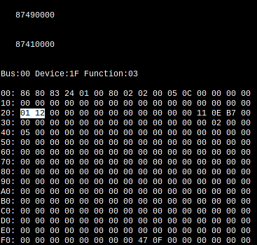
I have highlighted bytes 0x20 and 0x21 because they define the IO
Space base address of the device.
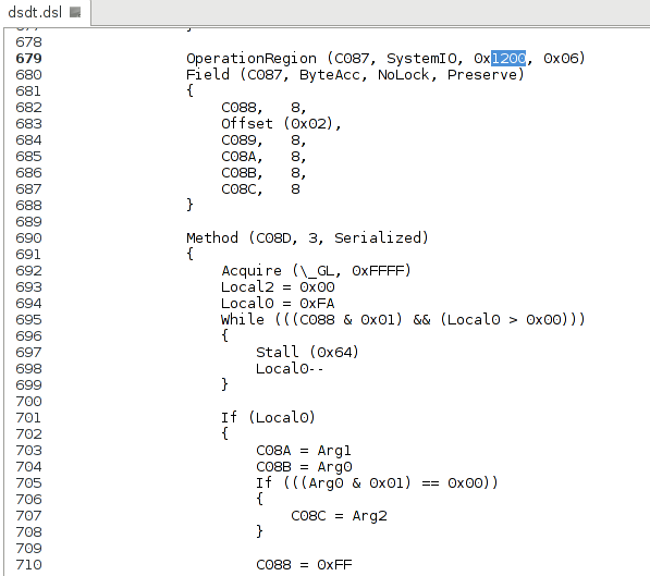
So, it's at IO port 0x1200.
$ cat /proc/ioports shows it there
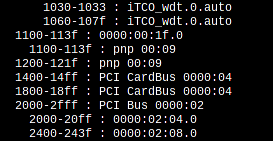
But is this even used by ACPI at all? Building on the knowledge
acquired in the previous bug I looked for 1200 in the dsdt.dsl
file that I had extracted before.
And yes, it is here, ACPI tells the linux kernel to reserve it as
a motherboard resource and not to use this address space for
anything else.
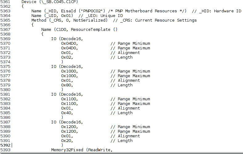
There is also the definition of an OperationRegion with variable
names, sizes and a method that uses them.
So, ACPI uses the device but, as we have seen, physically, only
the memories and the frequency generator are connected to it. The
SPD data is only needed once at boot up by the BIOS routines that
initialize the laptop. Changing whether certain clocks are active
is only done at power state changes.
The next step is dangerous (AND IT WILL VOID YOU WARRANTY, LOL)
in the sense that it may not be possible to securely suspend the
laptop afterwards but I considered the risk low enough to try
this.
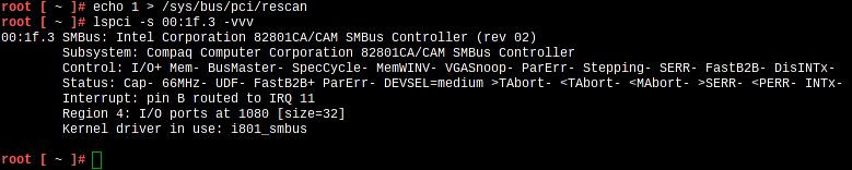
You will notice that the kernel changed the port number to 0x1080
and assigned a driver to the device.
And 'decode-dimms' works now.
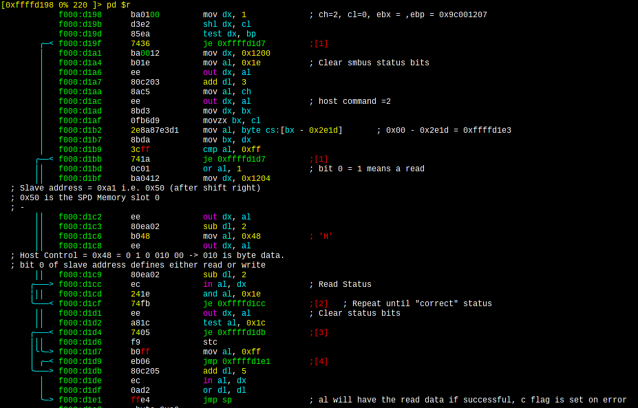
Just out of curiosity here are some BIOS routines...
The SMBus routine.
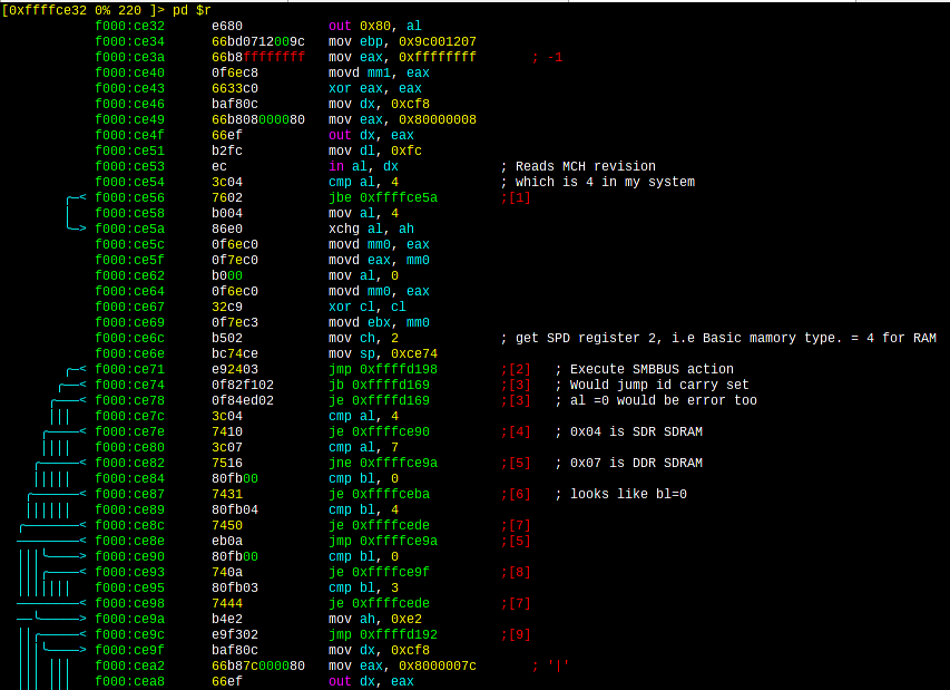
And the beginning of the MCH-M memory configuration routine
System EEPROM
Here it is, in page 22.
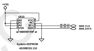
It is a NM24c02. I have found the respective datasheet.
This is a very common chip, in fact it is also the same that was
used by Kingston to hold the SPD data on the RAM DIMM.
All I know is that it connects to the Super-IO. I want to read the
data in there, but haven't been able to find any information about
this on the internet. There is this great blog post,
particularly this part that seems relevant, but not much more.
The EC has one additional function. The ACPI spec allows
for an i2c bus to be implemented through the EC, with EC registers
mapping to i2c registers. The observant among you will realise
that this means that there's an indexed access protocol being
implemented on top of indexed access hardware, which is more
layers of indirection than seem sane. For additional humour, this
is usually only used to add support for ACPI smart batteries. ACPI
batteries are generally abstracted behind a set of ACPI methods
that provide information. Smart batteries instead speak i2c
directly to the OS[2] for no real benefit. Linux handles these
devices fine, and while the chances are you probably don't have
one, the chances are also that if you do you haven't noticed.
My plan is to tackle this "bug" next when I manage to find some free
time.
Debugger in the BIOS
This is the result of running the strings command in the BIOS kept
at the low memory area addresses 0x000E0000 and forward.
lfs [ ~/Compaq Evo N610c ]$ strings
-tx fwh-000E0000-000FFFFF.bin | head -40
960 G b,#
97c I x8t
983 IB x8t
9de PCDB:
9e5 MD %<
a01 MM }?
a0f MK ?A
a55 BE $2I
a5c BD 2I
aac ^ Error
ab5
G [<offset>]
b30 Starts execution at the current
CS:EIP. Breaks at optional <offset>.
b77 G =<start> [<end>]
b8a Starts execution at
<start> offset. Breaks at optional <offset>.
bd1 Clears all breakpoints and
starts execution at current CS:EIP.
c13 T [<count>] [NOREGS]
c28 Executes one instruction at
current CS:EIP or executes <count> instructions.
c77 Specifying NOREGS will turn off
register dump for each instruction.
cbd SPecifying * for <count>
will trace until a breakpoint is triggered.
d04 TI [<count>] [NOREGS]
d1a Same as T but steps into INT
calls.
d40 P [<count>] [NOREGS]
d55 Same as T but steps over CALL,
LOOP and REP instructions.
d92 U [<addr>] [<end>]
da5 Disassemble code. If no
selector, CS is assumed. Breaks at optional <end>
df1 offset. Substituting a "$" for
<addr> will start from current CS:EIP.
e39 U [<addr>] [l<count>]
e4f Disassemble <count> lines
(hex).
e74 R [<reg> [<val>]]
e86 Display/modify CPU registers.
If <val> specified, it is written to <reg>.
ed2 DR [<reg> [<val>]]
ee5 Display/modify CPU debug
registers.
f0b SR [<reg> [<val>]]
f1e Display/modify CPU registers
saved in SMI RAM.
f52 Display CPU control registers.
f74 I<size> <port>
f83 O<size> <port> <val>
f98 Input/output data, where
<size> is B (8-bits), W (16-bits), or D (32-bits).
fe6 Output to port, where
<size> is B (8-bits), W (16-bits), or D (32-bits).
1032 PI<size> <bus> <device>
<func> <index>
It seems pretty obvious that there is a debugger / disassembler in
the BIOS.
The question is: how can this be activated? How can I run it?
This was my hardest hack as it was the one that took the longest.
But it was very interesting nonetheless.
It led me to this document. It contains
a very nice reference of the PC architecture BIOS calls/interrupts.
Another cool document is this
one, which is a PC-DOS / MS-DOS 3.30 technical reference, with a
good introduction and
a description of all the interrupts and function calls. There is
also a good description of the DEBUG command.
So, I was going around in radare2 trying to find any reference from
the "normal" BIOS at addresses 0xF0000- 0xFFFFF
onto addresses in the 0xE0000-0xEFFFF range but couldn't find any...
Then I looked at the disassembled code and tried
to find any piece of code that was relatively large and did not end
up with POPs and RET. Also unsuccessful. Then I
thought about randomly jumping into code in that region and see what
happened. This is why I started investing time in
understanding the DOS DEBUG command. Then by mere chance I was
scrolling up and down and saw this...
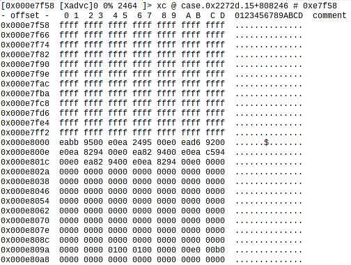
So... Lots of ffff followed by lots of 0000 with some stuff in
between.
A number of EAs in there, between the other numbers...
I had encountered EAs in disassembly before, so I knew these were
long jumps.
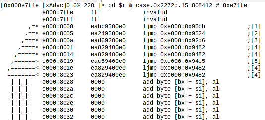
It was time to boot into DOS and try them out.
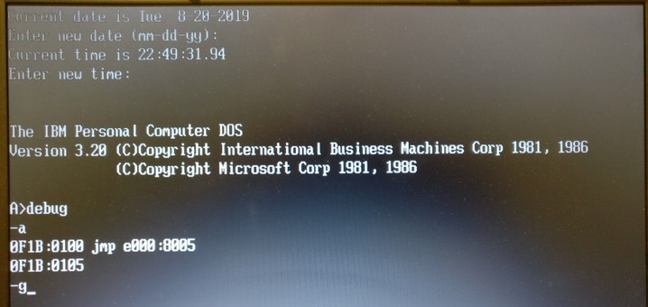
This will start the DEBUG command, assemble a jump instruction in
that memory location and then run it
(command g stands for go.)
Some of these locations would crash the computer, while others would
just restart it and I felt like I was back to
square one.
I noticed, however, that when jumping to E000:8005, like shown above
and just before the reset, the cursor would
change shape from an underline to a block. The blocky cursor would
then also be present at the top of the BIOS boot
splash screen which did not happen before. After rebooting the
computer N times and losing hope I simply pressed
the ENTER key at the splash screen with the blocky cursor and....
surprise surprise...
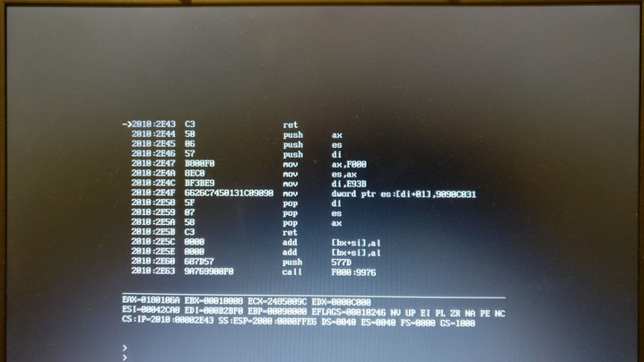
... I was presented with a prompt to the
monitor/disassembler/debugger program in the BIOS.
This is more advanced and has more commands (including help screens)
than the DOS DEBUG command but works in
a similar way. It allows you to disassemble, dump, look into
register values, do ins, outs, even look into and change
values in the PCI configuration space. You can also define
breakpoints.
If you are an operating system developer and/or if you want to hack
boot sectors and/or earlier initialisation boot
code this is very useful.
Update 7-Oct-2019
So, I made a boot sector like this...
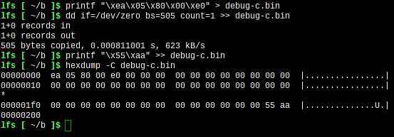
... and added an entry in grub.cfg
menuentry "Compaq BIOS debugger" {
set root=(hd0,1)
chainloader /boot/debug-c.bin
}
Now, every time I restart the laptop I have the option of starting
the debugger.
To spin or not
to spin that is the question
As I mentioned in the other
page about the computer, "Pentium4s ... get hot and spin the fans
too often."
This is definitely true and I tried to understand the logic behind
this and investigate why this is so.
So, I looked in the linux kernel sources and, buried there, there is
a small program called tmon, in the tools/thermal/tmon/ folder.
Compilation went smoothly and this is what I saw when I ran it.
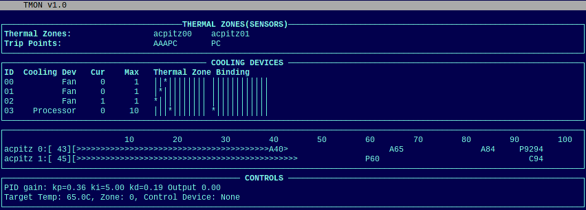
I'll let the README explain what the program is and what it does.
Increasingly, Linux is running on thermally
constrained devices. The simple
thermal relationship between processor and fan has become past for
modern
computers.
As hardware vendors cope with the thermal constraints on their
products, more
and more sensors are added, new cooling capabilities are
introduced. The
complexity of the thermal relationship can grow exponentially
among cooling
devices, zones, sensors, and trip points. They can also change
dynamically.
To expose such relationship to the userspace, Linux generic
thermal layer
introduced sysfs entry at /sys/class/thermal with a matrix of
symbolic
links, trip point bindings, and device instances. To traverse such
matrix by hand is not a trivial task. Testing is also difficult in
that
thermal conditions are often exception cases that hard to reach in
normal operations.
TMON is conceived as a tool to help visualize, tune, and test the
complex thermal subsystem.
What it does not explain is that the structures and values that the
kernel keeps in /sys/class/thermal end up
there as a result of the processing of the ACPI tables.
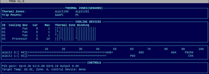
So, what we see is that there are 2 thermal zones (i.e. temperature
sensors) and their relationship with the
different "fans". We see also the current temperature reported by
each sensor (bars near the bottom) and the
temperatures that trigger the fans, i.e. the trip point bindings.
There aren't really 3 fans, what we have is a fan that can rotate at
3 different speeds.
The letters A, P and C stand for Active cooling (fan,) Passive
cooling (processor clock slow down) and Critical.
If you reach a critical temperature the system should shutdown to
protect itself.
tmon has another function, it allows you to manually switch the fans
on and off so manually select the speed as well.
What it does not let you do is change the thresholds.
So, we can see that, if the temperature is more that 50oC,
then the fan will start at the lower speed, when it reaches
60oC it increases the speed and then at 84oC
we get the higher speed.
On the way down, it will lower the speeds at 70oC, 55oC
and will switch it off at 40oC.
I did a number of experiments, switching the fans on and off and
realised that, completely idle, the processor
will naturally be at around 45oC or thereabouts. Left
alone, the system will naturally spin the fan at the lower speed
almost constantly, it will hardly ever reach 39oC.
Some of the earlier manuals of the laptop don't even mention the
2GHz Pentium4 and it occurred to me that maybe
Compaq did not change anything in the ACPI tables to account for the
different processors that ended up being
shipped with it.
So, as you can see in the backlight bug, I had already extracted and
decompiled the ACPI tables and could look into the
source code. I could still not fully understand it due to lack of
time and willpower to learn the language.
But that did not stop me looking on the internet for ways to change
the ACPI tables.
One of the first links that I clicked led me to this forum thread.
Lots of interesting and sad stories about people with really
buggy DSDT ACPI tables (DSDT is the table where the code is kept.)
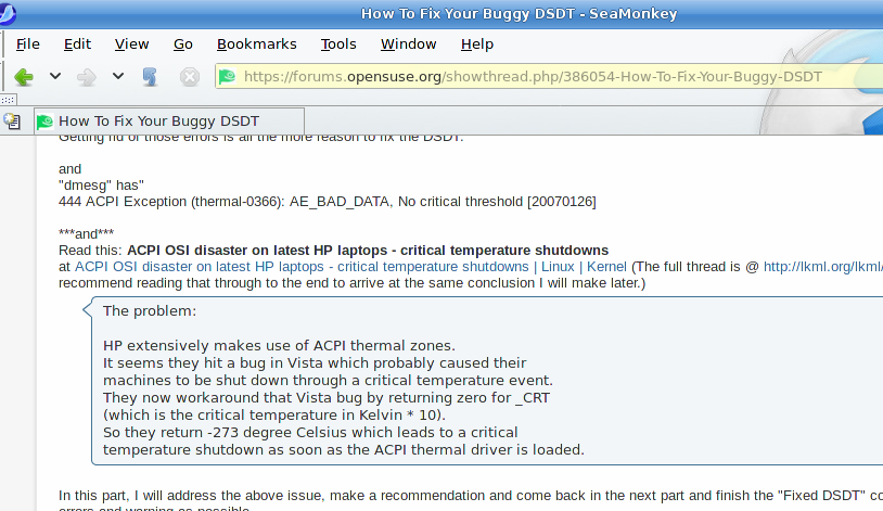
Two things caught my eye here. The first was the mention of a _CRT
value and the other that the temperature is in
Kelvin * 10.
I looked for _CRT in my DSDT
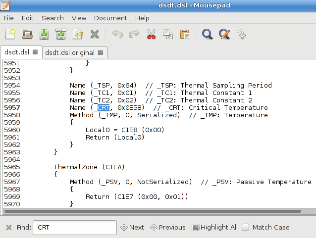
Sure enough, here it was.
0x0E58 is 3672 in decimal,
To convert from Kelvin to Celsius I subtracted by 2732 and divided
that by 10 which resulted in 94oC.
This was encouraging because this was the temperature I could see in
tmon.
Would it work the other way around? What value could I expect for 40oC,
55oC, etc...
As an example 40 *10 + 2732 = 3132 = 0x0C3C
Cool, it seems like all the temperatures I was looking for were
there, from line 5564 to line 5579
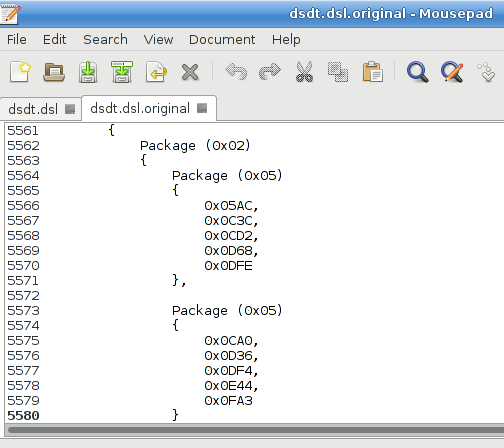
Time to change them.
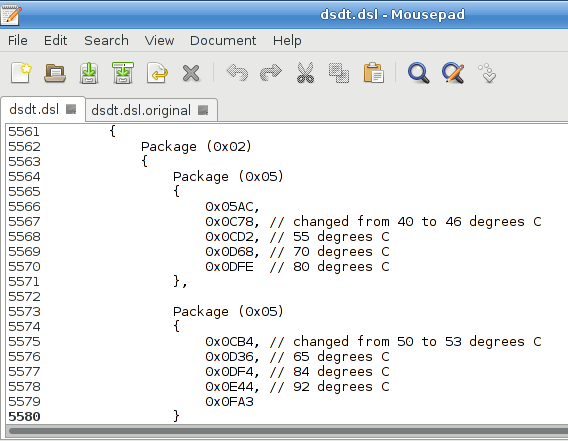
All that was left was to recompile the table with iasl and test it.
The kernel file /Documentation/acpi/dsdt-override.txt tells you how
to do it.
(It directs you to this
helpful article from intel.)
$ generate/unix/bin/iasl -tc -cr -vr dsdt.dsl
I then needed to edit the resulting DSDT.hex file and change the
name of the table to AmlCode
$ cp dsdt.hex /sources/linux-4.9.135/include/DSDT.hex
I ensured that...
CONFIG_STANDALONE=n
CONFIG_ACPI_CUSTOM_DSDT=y
CONFIG_ACPI_CUSTOM_DSDT_FILE="DSDT.hex"
... compiled a new kernel and it worked!!!
I had changed the thresholds successfully and the fan now spins only
sporadically.
The "Stupid Square
Thingy"
13-Apr-2020
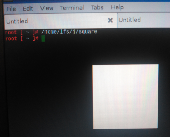
I'll start this one by showing the "solution" out right. Here it is,
in all it's glory... A white square in the screen.
"WOW, how did you do it?" you may ask in annoyed disbelief, thinking
to yourself internally "Why?!? WTF, FFS..."
So let me show you the code, maybe it will be a bit clearer then
#include <fcntl.h>
#include <errno.h>
#include <sys/mman.h>
#include <unistd.h>
#include "radeon_reg.h"
#define UV (unsigned long * volatile)
int main () {
int fd;
unsigned char * volatile r;
long temp;
fd=open("/sys/bus/pci/devices/0000:01:00.0/resource2",O_RDWR|O_CLOEXEC);
if(fd==-1) return errno;
r=mmap(NULL,64*1024,PROT_READ|PROT_WRITE,MAP_SHARED,fd,0);
if(r==MAP_FAILED) {r=NULL;close(fd);return errno;}
temp=*UV(r+RADEON_DP_GUI_MASTER_CNTL);
*UV(r+RADEON_DP_GUI_MASTER_CNTL)=RADEON_GMC_DST_PITCH_OFFSET_CNTL|
RADEON_GMC_BRUSH_SOLID_COLOR|(6<<8)|RADEON_GMC_SRC_DATATYPE_COLOR|
RADEON_ROP3_ONE|RADEON_GMC_CLR_CMP_CNTL_DIS;
*UV(r+RADEON_DST_X_Y)=(200 << 16) | 200;
*UV(r+RADEON_DST_WIDTH_HEIGHT)= (150 << 16) | 150;
*UV(r+RADEON_DP_GUI_MASTER_CNTL)=temp;
}
(To compile the program you'll also need this,
the radeon_reg.h file)
Still not clear?
I have no #includes for GTK, QT, wxWidgets, SDL, not even xcb or
xlib? What am I doing there?
So, it got stubbornly stuck into my mind that I had to be capable of
using the 2D accelaration functionality of the Radeon and that I
could not stop until I did it. This had to be done directly on the
card. That square is the result of that.
But what is a video card anyway? There are some things that are
common to all of them:
- At least one "connector" to a display, in my laptop I actually
have 4, the LCD, the VGA port, S-Video port and the DVI port if
I use the port replicator.
- A way to access memory, in my case I have 32megabytes of
dedicated Video RAM, which connect directly to the M7 chip
- At least one internal circuit that can read from that memory
and create the signals necessary to drive the display units
through the connectors. For historical reasons these are called
CRTCs. The M7 has 2 of these, I can see images in any
combination of 2 ports out of the 4.
Graphics cards are inside the computers but are different animals
altogether. They are pets of the main processor and have to follow
its orders. It is the pentium4 that tells the card what to display
on the screen. The card also has to have a way to be told what to
do.
Part 1)
So I had to do research.
This was a quite a roller coaster... To get there I had to do a lot
of "internet". I started with the R128
manual. As I said in the cracking the N610 page, this manual
"goes into a lot of detail, describing the architecture of the ATI
cards."
And this is true, up to a point. You get a good idea of how that
card works but just a very general idea of how the other ATI cards
do. I have a R100, M7, an ATI 7500, based on another chip. The
examples in that just do not work.
The R128 manual tells us to read the "Programmer's Guide to
the EGA, VGA, and Super VGA Cards" by Richard Ferraro to understand
more about the VGA Controller mode. At first I could not find it
anywhere on the internet but then I found it here.
At first I gave up as it wouldn't download but one day I was patient
enough to wait for the page to load and then was happily surprised.
This is a pdf file which is a brilliant scan of the original paper
book. The OCR is amazing, all the pages are there. You have the
original jpegs of each page and overlaid on it you have the text
that you can copy and search. At 1612 pages we end up with a 485Mb
file. So this is the second reason I'm not hosting this file. The
first is that the book is still being sold online, even though it
came out in 1994. And I can also understand why, it is a brilliant
book, it tells you the history of graphics on the PC from the MDA,
CGA, Hercules, EGA, VGA and the absolute explosion of the Super VGA
cards. Along the way it explains all there is to know about frame
buffers, colour palettes, resolutions, coordinates, text, graphics,
fonts, drawing lines, solids, "blits", registers, etc, etc. Everyone
trying to understand graphics cards needs to read this book. It's
that strong. You also end up understanding what 2D acceleration is.
So, why is there no documentation for the M7 chip inside my Compaq?
The Ferraro book tells us about 13 different companies competing in
the graphics card market in 1993/1994: IBM, ATI, C&T, Cirrus
Logic, Video7, IIT, NCR, OAK, S3, Trident, Tseng Labs, Paradise and
Weitek. (Ndivia is still absent, interestingly). These companies
were all fighting to be the best and a climate of secrecy ruled. In
the pre win95 days companies would associate themselves with
software developement houses which could then develop the sw that
made use of the best features of the cards. Non Disclosure
Agreements had to be signed in order to have access to
documentation, all to prevent the competition from stealing their
best ideas. Alternatively, the companies would provide software
developer kits with defined Application Programmer's Interfaces that
allowed programming the cards. Importantly, the cards also strived
to implement in hardware as much of the MS windows 3 functionality
as possible. Developing drivers for windows was the exclusive
responsibility of the card manufacturer. The other huge market was
DOS games.
This was a problem for linux with its GPL rules when it became more
prominent in the early 2000.
The development of the linux drivers for the ATI cards was at first
ignored by ATI, but then, later, ATI/AMD engineers actively
participated in the drivers' development.
Nowadays we see that none of those companies survived. ATI was
bought by AMD in 2006. Intel collaborated with Tugsten Graphics, the
company behind the development of much of the linux 3D code. Nvidia
came from behind and is obviously still around.
From 2007/2008 AMD and Intel decided to release practically all of
the documentation concerning their cards. Unfortunately, I guess due
to legalities, the information for the older cards like mine is not
publicly available.
(Don't quote me on any of this, it's all very sketchy and hush
hush on the internet...)
So, where could I find more??? Well, the whole linux graphics stack
software was at my disposal so I started trying to understand it.
I had to read:
- This very good overview
http://moi.vonos.net/linux/graphics-stack/
- This document from the author of the nouveau driver
linuxgraphicsdrivers.pdf
- The Wikipedia articles starting from here
https://en.wikipedia.org/wiki/Direct_Rendering_Manager
- Stuff from X.ORG itself, of course
https://www.x.org/wiki/Development/Documentation/HowVideoCardsWork/
- More stuff from freedesktop.org
A bit of history https://dri.freedesktop.org/wiki/DriHistory/
https://dri.freedesktop.org/wiki/RadeonArchitecture/
I also came across a little program called Radeontool which REALLY
helped a lot.
Part 2)
The Mobility Radeon is a PCI device, therefore it has a PCI
configuration space that can be queried.
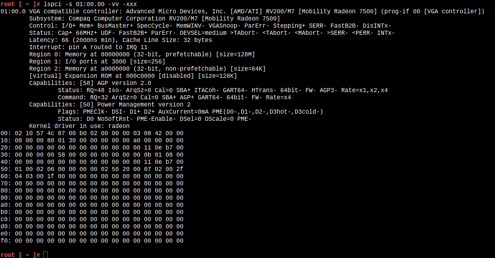
The linux kernel enumerator, when the kernel starts, finds it in bus
1, device 0, function 0.
In the hex dump we can see the device vendor 1002 and the device id
4c57.
The device is being controlled by the kernel device driver called
"radeon".
The rest of the fields were decoded by the lspci utility and are
shown above. Of most interest are the three "Regions".
The pci configuration space has "told" the kernel that it needed a
region of I/O space of 256 bytes, a "memory" region of 64Kbytes and
another of 128Mbytes. The kernel has then assigned the addresses of
3000h, A0000000h and 80000000h respectively.
The differences between "I/O" and "memory" address spaces are
documented in chapter 12 of volume
1 of the Intel manual. If you don't understand what they are
yet, reading this is required.
The linux kernel provides these spaces as abstractions in the
filesystem and this means that I can "open" then as files.
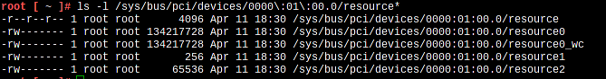
So now you understand the 1st line of the program with the open
statement. I can access that physical space using file related
functions, like read, write, seek... But there is another, better
way...
To understand the 2nd line, one has to read chapters 1, 2 and 3 of volume 3 of the Intel
manual. (A lot of pages, all worth it.)
This picture will help a bit.
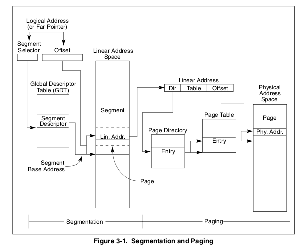
It can be summarised as follows. Any program running on a x86
processor in protected mode, (which is the one used by linux,) when
addressing memory using any of the mov instructions, will do so
using a value which is a pointer to the addressed byte. That pointer
has 2 parts, a segment selector and an offset. The segment selector
points to a table and is used as an index into it. That table
contains values for each possible index. That value is then added to
the offset to create a new pointer. That pointer is what the
application knows and uses in it's "personal" "linear" address
space.
But, in linux, paging is also used, so the value calculated before
is not used to address physical memory but instead is used as
another pointer into the paging tables. These tables are an extra
layer of indirection, they are maintained by the operating system
and, at last, we have the physical address.
The physical address is actually what the Pentium4 outputs in
its address lines in the front side bus to the MCH-M northbridge.
So, this is what the mmap function does. In this case, it is a
mechanism that returns to the application, a pointer to a physical
memory area, by means of creating the necessary entries in the
paging tables.
I got there by analysing the source code of Radeontool and libpciaccess,
which it uses.
In this example the values b7712000 and af552000 were returned to
the application. Writing to these addresses directs the writes to
the resource2 and resource0 areas and ultimately to the graphics
card.
What are these areas? These are explained well in the Radeon
Architecture article that I link to above.
Let me quote from that:
"
It is important to note that EVERYTHING you are doing to radeon card
ultimately boils down to a series of register writes. The X server
basically takes the high level functions and translates them into a
series of register writes. Mesa takes the OpenGL commands and
(working with DRI) translates them into a series of register writes.
"
Resource2 are all the registers that control the card, their names
and functions are described in the M6 Registers
document. I don't have the corresponding M7 document, but the radeon
cards evolved keeping always a big level of register compatibility
and all the required registers are actually also in the kernel and
Xorg drivers: you'll find radeon_reg.h linked above. All registers
have names and some registers can be accessed by more than one way.
Here are a couple of examples:
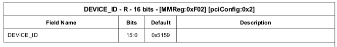
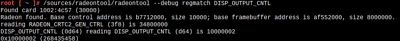
So, the document tells us that the DEVICE_ID register exists both in
the pci configuration space and in the Memory Mapped Register space.
We had already seen the value 4c57 in the lspci printout and I
managed to verify it with the radeontool.

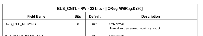
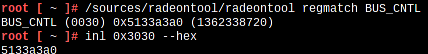
Let's see another example. In this one I query a register which
exists in both the MM and IO areas.
So now all the other statements in my program can be understood.
All that I do is read and write from and to the registers.
But how did I know which registers to write to, to draw the square?
The clue is in the HowVideoCardsWork link above.
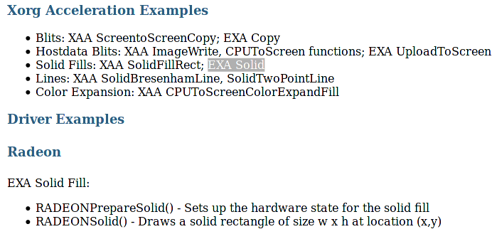
In the source code of the Xorg driver (xf86-video-ati-7.7.0) there
is a file called radeon_exa_funcs.c and there we see the
RADEONPrepareSolid and RADEONSolid functions. I studied the code and
took only the minimum required:
Change RADEON_DP_GUI_MASTER_CNTL,
then RADEON_DST_X_Y and then
RADEON_DST_WIDTH_HEIGHT. In
the end I put back the value of the RADEON_DP_GUI_MASTER_CNTL
register. It runs so quickly that I do not disturb the status of the
X server driver in any way, except, of course, now I have a white
square thingy on the screen. This is pretty harmless, it goes away
anytime the window is updated.
But, is this enough to fully understand the card? NO!! Lots of
questions remain:
- How do you change the card from VGA compatibility mode to
Accelerator mode?
- How does the card work with Colours? And Text Fonts? And Icons?
And the mouse pointer?
- What is this Composite Mode that allows some windows to be
transparent?
- How does the Memory Mapping AGP GART device works? How does the
card use PCI Bus mastering?
- What is the Command Processor and how does it work?
- What are the 3D capabilities of the card? How do you use them?
- What's up with programs that play video? What do they do
differently?
- How about multi monitor setups, i2c / EDID? Resolutions?
Horizontal / vertical synch?
The "Stupid Square
Thingy" - slow and steady
2020-06-10
This time I did things differently. I did not look at any code from
the linux radeon drivers.
So, I already knew that the registers are PCI resource2 and that the
video card memory is mapped in resource0.
But, how could I write to it so that I could draw a square on the
screen?
I started with my friend crappy here...
// Crappy Stupid Square Thingy
#include <stdio.h>
#include <fcntl.h>
#include <errno.h>
#include <sys/mman.h>
#include <unistd.h>
#include "radeon_reg.h"
#define UV (unsigned long * volatile)
int main () {
int fd;
unsigned int i;
unsigned char * volatile r;
long temp;
fd=open("/sys/bus/pci/devices/0000:01:00.0/resource0",O_RDWR|O_CLOEXEC);
if(fd==-1) { perror("1"); return errno; }
r=mmap(NULL,64*1024*1024,PROT_READ|PROT_WRITE,MAP_SHARED,fd,0);
if(r==MAP_FAILED) { r=NULL; close(fd); perror("2");
return errno; }
for(i=1*1024*1024+32*1024+64;i<5*1024*1024;i+=4)
*UV(r+i) = 0xffffffff;
}
So, I just poked values using a for loop, changing the initial and
final values until I found the area of video memory
from where the M7 is getting what is being displayed on the screen.
In this case, we can see that it starts 1M and 32Kbytes into the
memory. (The +64 is just for show.)
This is 0x00108000 in hexadecimal.
That's all well and neat and all that but, I wasn't really happy
with this.
I dug into the radeon_reg.h file, into the register description pdf
and into and into the Rage 128 Developer's guide
until I found the CRTC_OFFSET register. Then the radeontool
confirmed the value. Bingo!
root [ ~ ]# /sources/radeontool/radeontool
regmatch CRTC_OFFSET
CRTC_OFFSET (0224) 0x00108000 (1081344)
Time to use my newly acquired knowledge and waste my time writing
another useless program.
// Stupid Square Thingy 2
#include <stdio.h>
#include <fcntl.h>
#include <errno.h>
#include <sys/mman.h>
#include <sys/stat.h>
#include <unistd.h>
#include "radeon_reg.h"
#define UV (unsigned long * volatile)
int main () {
int fd0, fd1;
struct stat s;
unsigned char * volatile m;
unsigned char * volatile r;
long co; // crtc_offset
int x1,y1,x2,y2,x,y,b;
int bypp; //bytes per pixel
int ppl; //pixels per line
fd0=open("/sys/bus/pci/devices/0000:01:00.0/resource0",O_RDWR|O_CLOEXEC);
if(fd0==-1) { perror("resource0 open"); return errno;}
if (fstat(fd0, &s) == -1) { close(fd0);
perror("fstat0"); return errno; }
m=mmap(NULL,s.st_size,PROT_READ|PROT_WRITE,MAP_SHARED,fd0,0);
if(m==MAP_FAILED) { close(fd0); perror("resource0 mmap");
return errno; }
fd1=open("/sys/bus/pci/devices/0000:01:00.0/resource2",O_RDWR|O_CLOEXEC);
if(fd1==-1) { perror("resource0 open"); return errno;}
if (fstat(fd1, &s) == -1) { close(fd1);
perror("fstat2"); return errno; }
r=mmap(NULL,s.st_size,PROT_READ|PROT_WRITE,MAP_SHARED,fd1,0);
if(r==MAP_FAILED) { close(fd1); perror("resource2 mmap");
return errno; }
co=*UV(r+RADEON_CRTC_OFFSET); //screen location in video
memory
bypp=(*UV(r+RADEON_CRTC_GEN_CNTL) &
RADEON_CRTC2_PIX_WIDTH_MASK ) >> 8;
switch (bypp) { //from the M6 register manual, page 218
case 2: bypp=1; break;
case 3: bypp=2; break;
case 4: bypp=2; break;
case 5: bypp=3; break;
case 6: bypp=4; break; // This is still a 24bit
per pixel mode
// with 256 shades of red, blue or green.
// The 4th byte is ignored and wasted.
// However this mode is the fastest
// because in the x86 32 bits architecture
// memory acesses are always 4 bytes wide
case 7: bypp=2; break;
case 8: bypp=2; break;
default: 4;
}
ppl=(*UV(r+RADEON_CRTC_PITCH)& 0X3ff)*8;
//see Ferraro's book to understand pitch
x1=200; y1=200; x2=350; y2=350; //where's my square at?
for (y=y1;y<y2;y++) {
for(x=x1;x<x2;x++) {
if (bypp==4)
*UV(m+co+y*ppl*bypp+x*bypp)=0x00FFFFFF;
else
for(b=0;b<bypp;b++)
{
*UV(m+co+y*ppl*bypp+x*bypp+b)=0xFF;
}
}
}
}
And here are the results
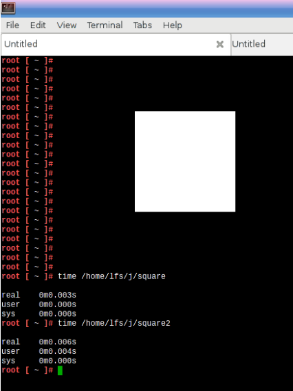
This extremely unscientific method shows that the second way of
drawing the square takes twice as long.
FreeDOS and the PCI BIOS bug
2021-08-08
I wrote back here that "In
a way, this laptop is the perfect study object, as it comes from a
time that married the old ISA (and Plug&Play)
computers with the more modern ACPI / PCI ones of today" but, to be
honest I was not really sure how a computer designed with Windows XP
in mind would behave with older software. I had already toyed with
MS-DOS 3.2 so I went looking for something else.
So, what about Freedos?
I had heard of FreeDOS but never really attempted to discover more.
Who needs DOS when you already have a free Linux
distribution running on your computer? However, upon reading that
"...all FreeDOS programs are distributed under the GNU General
Public License or a similar Open source software license" it
really piqued my interest.
So, how do you install Freedos? The typical way is to use a virtual
machine and this is exactly how I started. I created a virtual hard
drive image and used the stable cd-rom image which I had downloaded
from the FreeDOS website.
This went smoothly but very slowly. The installation gives you the
option to install source code, which is great.
After reboot you are left with the famous C:\> prompt and a
display of the memory map. The boot process also presents you a list
of 4 different memory managers and configurations to choose from.
And you start exploring from there. The wiki is also great and you
soon learn about the package manager FDIMPLES (in FD1.2 install it
first with fdinst install d:\utils\fdimples.zip) and the FDNPKG
package updater that downloads and install new versions of programs
from the internet.
This was a surprise for me. I wasn't expecting FreeDOS to be so
"evolved". You also have a program called FDAPM that halts the
processor when in idle. FreeDOS supports long file names, FAT32 and
reports itself to programs as DOS version 7.10.
All in all this is a modern distribution and full of features.
So, the next step was to install it to the hard drive and dual boot
with Linux From Scratch using Grub.
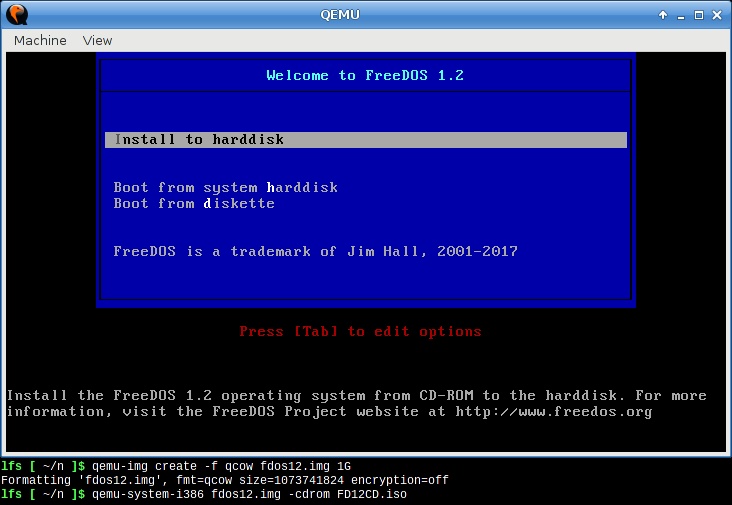
I created a blank dos partition in the hard drive, downloaded
FreeDOS 1.3rc4 and, not wanting to waste a CD-ROM, took advantage of
QEMU and did this...
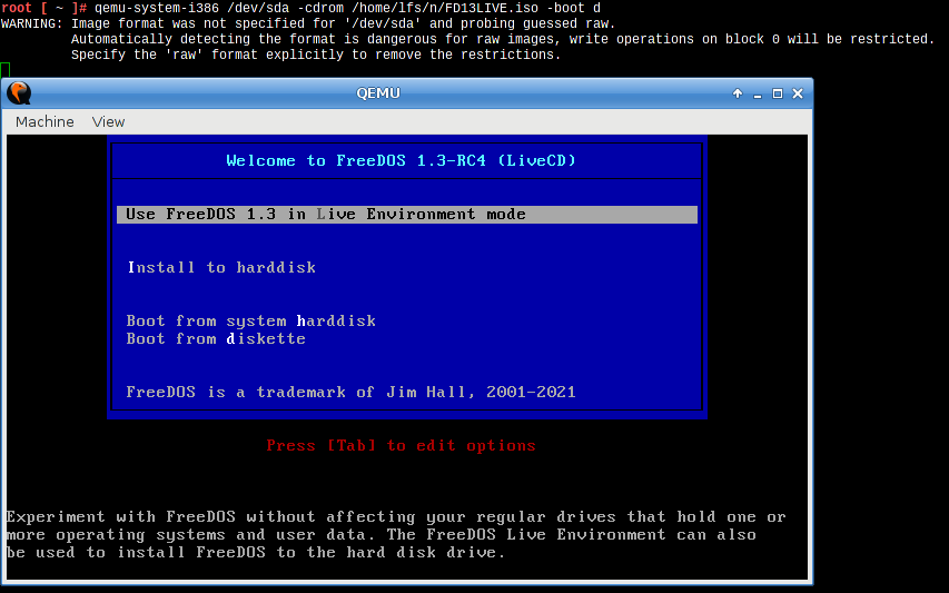
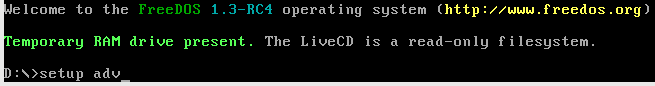
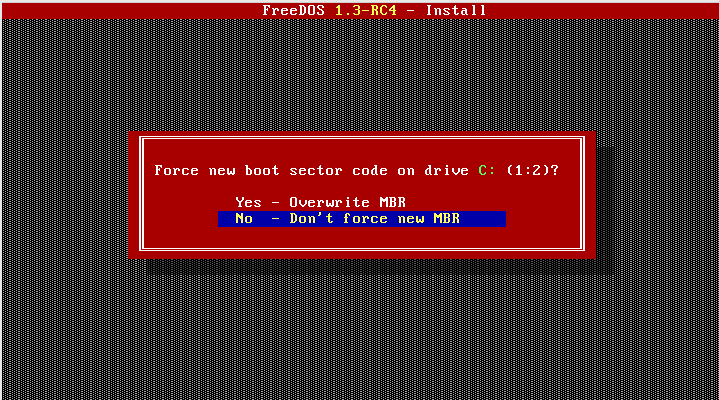
You need to be root to do this. It's risky but it works. The trick
here is to boot to the live environment, then run "setup adv"
You will be in a new nice advanced installer that, at one point,
asks you if you want to overwrite the MBR. The answer here is
obviously "no" so that you do not destroy the GRUB installation.
After that, all that was left was to update /boot/grub/grub.cfg
withmenuentry "Freedos 1.3rc4" {
set
root=(hd0,2)
chainloader +1
}
Transferring new files to the DOS partition from Linux is easy, just
mount it to a folder and copy away. The fist 2 things I transferred
were the FD13LIVE.ISO and FD13BNS.ISO files and a copy of
SHSUCDHD.EXE which, strangely, is not part of the distribution but
can be found on the site of the package creator.
I kept playing with FreeDOS, installing and removing stuff and this
is the pinnacle of my achievements:

Browsing the internet in Arachne using a Wireless LAN Orinoco PCMCIA
card.
Speaking of playing, FreeDOS also comes with lots of games and... to
my dismay... a lot of the more complicated ones did not run
correctly. I would see nothing but a black screen. This was very
annoying, how could this be? Was this a FreeDOS or a Compaq problem?
Surely it could not be FreeDOS, the games were part of the
distribution itself.
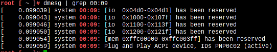
I kept thinking about this and then I remembered something, these
lines in dmesg
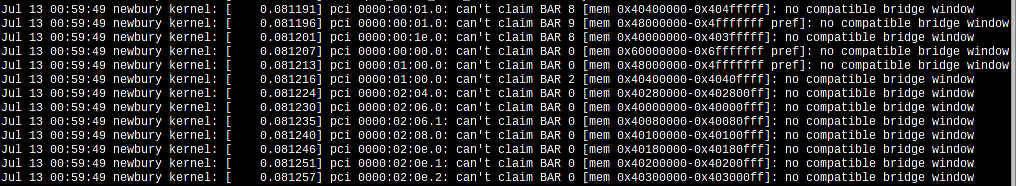
What this means is that, while initializing, the Linux kernel reads
the PCI configuration space, finds these addresses there and
realises that they are wrong. Later on, it completely reconfigures
all de devices to other addresses.
The reason why they are wrong is because I have 2GBytes of RAM on
the laptop so, my RAM goes from 0x00000000 to 0x80000000. The BIOS
is leaving the graphics card, the PCI and PCCard bridges and the USB
controllers configured for addresses conflicting with RAM. This is a
serious bug.
Linux is smart enough to realise this and fix it before passing the
devices to their respective drivers but there is no such luck with
DOS.
To test this I simply removed one of the 1Gbyte DIMM sticks and all
the FreeDOS games started working properly.
How could I fix this? I did not want to have to remove a memory
stick every time I wanted to play a a game...
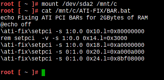
I remembered how, in Linux you have the command setpci, which is
part of the pciutils package.
Searching the net, I ended up here which shows us how to
compile setpci and lspci for DOS. As a bonus, you also end up with a
cross compiler. A very neat setup...
And here is the solution. I wrote a batch file that changes the
addresses of the AGP Bridge and the Radeon graphics card to
addresses above 2Gbytes.
But, could I still do better than this? As it turns out, I could,
and I did...
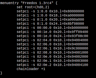
... because GRUB also has a setpci command.
(Comments on this page are welcome - please email me at
compaq(a.t.)edbatalha.info )
